Highlights
•The thickness of graphene grown on SiC was determined by AES depth profiling.
•The AES depth profiling verified the presence of buffer layer on SiC.
•The presence of unsaturated Si bonds in the buffer layer has been shown.
•Using multipoint analysis thickness distribution of the graphene on [...]
PAM-XIAMEN is able to supply you with P type SiC substrate, more specifications please see: https://www.powerwaywafer.com/p-type-silicon-carbide-substrate-and-igbt-devices.html.
SiC single crystal has the characteristics of wide bandgap, high critical breakdown electric field, high thermal conductivity, high carrier saturation drift speed, and good stability. Among the numerous crystal [...]
2024-04-19мета-автор
PAM XIAMEN offers 4″ Silicon Wafer.
Diameter
Type
Dopant
Growth
method
Orientation
Resistivity
Thickness
Surface
Grade
100
P
Boron
CZ
-100
1-20
43768
P/P
PRIME
100
P
Boron
CZ
-100
1-20
40-60
P/P
PRIME
100
P
Boron
CZ
-100
1-20
80-100
P/P
PRIME
100
P
Boron
CZ
-100
1-20
180-200
P/P
PRIME
100
P
Boron
CZ
-100
1-20
300-350
P/E
PRIME
100
P
Boron
CZ
-100
1-20
300-350
P/P
PRIME
100
P
Boron
CZ
-100
1-20
350-400
P/P
PRIME
100
P
Boron
CZ
-100
1-20
375-425
P/E
PRIME
100
P
Boron
CZ
-100
.001-.005
450-500
P/P
PRIME
100
P
Boron
CZ
-100
.005-.02
450-500
P/P
PRIME
100
P
Boron
FZ
-100
>3000
450-500
P/P
PRIME
100
P
Boron
CZ
-100
1-20
450-500
P/P
PRIME
100
P
Boron
CZ
-100
.001-.005
500-550
P/E
PRIME
100
P
Boron
CZ
-100
.005-.02
500-550
P/E
PRIME
100
P
Boron
FZ
-100
>3000
500-550
P/E
PRIME
100
P
Boron
CZ
-100
1-20
500-550
P/E
PRIME
100
P
Boron
CZ
-100
1-20
500-550
P/E/DTOx
PRIME
100
P
Boron
CZ
-100
1-20
500-550
P/E/Ni
PRIME
100
P
Boron
CZ
-100
1-20
500-550
P/E/WTOx
100
P
Boron
CZ
-100
1-20
950-1050
P/E
PRIME
100
P
Boron
CZ
-100
1-20
950-1050
P/P
PRIME
For more information, please visit our website: https://www.powerwaywafer.com,
send us email at sales@powerwaywafer.com and powerwaymaterial@gmail.com
Found in 1990, Xiamen Powerway Advanced Material Co., Ltd (PAM-XIAMEN) is a leading manufacturer of semiconductor material in China.PAM-XIAMEN develops advanced crystal growth and epitaxy technologies, [...]
2019-03-04мета-автор
PAM XIAMEN offers Thermal Oxide Wafers, 2 – 4″ Research Grade.
Thermal oxide or silicon dioxide layer is formed on bare silicon surface at temperature range from 900°C ~ 1200°C . Compared to CVD deposited oxide layer, thermal oxide has a higher uniformity, and [...]
2019-05-20мета-автор
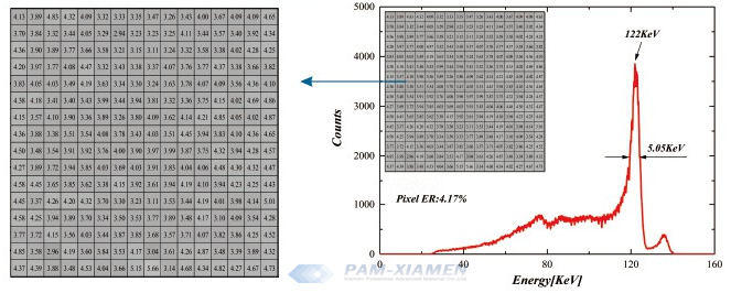
1.Introduction of CZT Portable Spectrum Analyzer
CZT_PES01 is used for nuclides identification.
It was designed to work with CZT detectors.
The instrument integrated low noise preamplifier,
shaping amplifier, high voltage, DMAC, software and LED screen.
A battery also built in it.
2.Technique data of CZT Portable Spectrum [...]
2021-03-02мета-автор
PAM-XIAMEN is able to supply epitaxial thin film of P-type GaN on GaN substrate. P-type GaN thin film epitaxial on GaN substrate is the main technique for developing emitting device. Mg is the most common p-type dopant in III-nitride material systems, partly due to the [...]
2021-12-23мета-автор