PAM XIAMEN предлагает кремниевые пластины с нитридным покрытием.
Stoichiometric LPCVD Nitride on Silicon Wafer Specification
Диапазон толщины: 100Å - 4500Å
Обрабатываемые стороны: обе
Показатель преломления: 2,00 +/-. 05 @ 632 нм
Напряжение пленки: растягивающее напряжение> 800 МПа
Размер пластины: 1 ″ -12 ″ дюймов
Температура: 800С °
Газы: дихлорсилан, аммиак
Оборудование: горизонтальная вакуумная печь.
Нитрид
LPCVD
PECVD
Стохиометрический
Низкое напряжение
Сверхнизкое напряжение
More specifications of silicon nitride wafer by LPCVD please refer to https://www.powerwaywafer.com/silicon-nitride-wafer-si3n4-thin-film-by-lpcvd.html.
1. About LPCVD
Low-pressure chemical vapor deposition (Low-pressure CVD, LPCVD) is designed to reduce the operating pressure of the reaction gas in the reactor for deposition reaction to below about 133Pa. The LPCVD pressure drops below about 133Pa. Correspondingly, the free path of molecules and the gas diffusion coefficient increase, so that the mass transfer rate of gaseous reactants and by-products is accelerated, and the reaction rate of film formation is increased. When the chip spacing is reduced to 5~10mm, the mass transfer limitation can still be ignored compared with the chemical reaction rate of the chip surface, which creates conditions for vertical densely packed chips, and greatly increases the amount of chips loaded in each batch. The figure below is a schematic diagram of the LPCVD system:
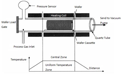
LPCVD Reaction Structure
LPCVD is the mainstream process for film deposition above 90nm. Films deposited by LPCVD will have better step coverage, good composition and structure control, high deposition rate and output. Furthermore, LPCVD does not require carrier gas, thus greatly reducing the source of particle pollution, and is widely used in the high value-added semiconductor industry for thin film deposition. LPCVD is widely used in silicon dioxide (LTO TEOS), silicon nitride (low stress) (Si3N4), polysilicon (LP-POLY), phosphosilicate glass (BSG), borophosphosilicate glass (BPSG), doped polysilicon, graphite alkenes, carbon nanotubes and other thin films.
2. FAQ about Stoichiometric LPCVD Nitride on Silicon Wafers
Q: «Наша лаборатория планирует изготовить волновод из нитрида кремния. поэтому нам нужно купить пластины нитрида кремния, а это значит, что нам нужны стехиометрические пленки нитрида кремния толщиной около 150 нм на пластинах из термически оксидов кремния. слой термического оксида должен иметь толщину не менее 1 мкм. Силиконовая подложка является гибкой. Нижняя пластина - это для нас хорошая термооксидная пластина. Есть ли у вас услуги обработки для выращивания 150 нм нитрида кремния с низким давлением LPCVD на подложке ниже? Спасибо.
Диаметр 100мм
Высший сорт, ССП
P-тип, легирующая примесь B
Ориентация <110>
Удельное сопротивление 1-10 Ом · см
Толщина 500 мкм
С влажным термическим оксидом 1000 нм »
A: 100mm P/B <100> 1-10 ohm-cm 500um SSP Prim Grade with 1um of Oxide and 150 nm LPCVD low stress silicon

For more information, please contact us email at victorchan@powerwaywafer.com и powerwaymaterial@gmail.com.