PAM-XIAMEN offers 4inch Semi-insulating GaAs Substrate with good flatness such as TTV<=3UM, BOW<=4um, and WARP<5um, TIR(Total Indicated Runout)<=3um, LFPD(Local Focal Plane Deviation)<=1um, LTV(Local Thickness Variation)<=1.5um, which can be used for Microelectronic application.
1. Specification of Semi-insulating GaAs Substrate
1.1 Semi-insulated GaAs Substrate PAM190425-GAAS
| Parameter | Customer’sRequirements | Guaranteed/Actual Values | UOM | |
| GrowthMethod: | VGF | VGF | — | |
| ConductType:. | S-I-N | S-I-N | — | |
| Dopant: | c doped | c doped | ||
| Diameter: | 100.0±0.2 | 100.0±0.2 | mm | |
| Orientation: | (100)±0.30offtoward (110) | (100)±0.30offtoward (110) | — | |
| OFlocation/length: | EJ|0-1-1|±0.50/32.5±1.0 | EJ[0-1-1]±0.50/32.5±1.0 | — | |
| IFlocation/length: | EJ|0-11|±0.50/18.0±1.0 | EJ[0-11|±0.50/18.0±1.0 | — | |
| Resistivity: | Min:0.6E8 | Min:0.8E8 | Max:2.4E8 | ohm.cm |
| Mobility: | Min:4500 | Min:4769 | Max:6571 | cm2/v.s |
| EPD: | Max:10000 | Min:700 | Max:700 | /cm2 |
| Thickness: | 600±25 | 600±25 | pm | |
| Bow: | Max:4 | Max:4 | μm | |
| Warp: | Max:5 | Max:5 | μm | |
| TTV: | Max:3 | Max:3 | μm | |
| TIR:. | Max:3 | Max:3 | pm | |
| LFPD: | Max:1 | Max:1 | pm | |
| LTV: | Max:1.5 | Max:1.5 | μm | |
| PLTV: | >90@15mm*15mm | >90@15mm*15mm | % | |
| ParticalCount: | <100/wafer(for particle>0.28um); Haze<5ppm |
<I00/wafer(for particle>0.28um); Haze<5ppm |
— | |
| EdgeRounding: | 0.375 | 0.375 | mmR | |
| Laser Marking: | Backside | Backside | — | |
| SurfaceFinish- front: |
Polished | Polished | — | |
| SurfaceFinish -back: |
Polished | Polished | — | |
1.2 VGF Semi-insulating GaAs Substrates PAM211206-GAAS
| Parameter | Value | UOM |
| Crystal growth method | VGF | |
| Crystal orientation | 100 | |
| Conduction Type | N-type, semi-insulating | |
| Dopant | c doped | |
| Resistivity @ 22 degree C | xx | cm |
| Radial resistivity variation | </=30 | % |
| Mobility min | xx | cm2/Vs |
| EPD max( average over wafer) | 1.0 E5 | cm-2 |
| Carbon concentration | xx | cm-3 |
| Bor concentration | xx | cm-3 |
| Diameter | 76,2+/-0,1 | mm |
| Flat System | SEMI-EJ | |
| OF | (0-1-1) | |
| Orientation tolerance OF | + / – 1.0 | degree |
| Length OF | 22.0+/-2.0 | mm |
| IF | (0-11) | |
| Orientation tolerance IF | + / – 2.0 | degree |
| Length IF | 11.0 +/-2.0 | mm |
| Surface Orientation | 100 | |
| Off orintation and tolerance | 0+/-0.25 | degree |
| Edge Rounding | Bevelled SEMI-M9 | |
| Thickness | 625+/-25 | um |
| Front side | polished, epi-ready (shelf-life 6 months) | |
| Edge exclusion | 5 | mm |
| TTV max | 6 | um |
| TIR max | 5 | um |
| Bow max | 8 | um |
| Warp max | 8 | um |
| LFPD (15x15mm field size) | xx | um |
| Particles ( diam >/=0.3 um) | xx | pcs/wafer |
Notes for double side polished:
Double side polished is not equal epi-ready on both sides. Backside polished not equal to epi-ready, front side polished by CMP, which is epi-ready, backside is only optical polished, can not be epi-ready, normally backside surface guarantee Ra<1nm, but front side should be Ra<0.5nm. so compared with front side, backside is matte, even if it is polished.
2. What is the Typical Carrier Concentration for Semi-insulating GaAs Substrate?
The carrier concentration for Semi-insulating GaAs wafer is E6-E7/cm3, typical value 6.71E6/cm3~1.12E7/cm3, please see below detail parmeters:
| Item No. | 4# | 91# | ||||
| Spec. | resistivity | mobility | C.C | resistivity | mobility | C.C |
| 1 | 1.32E+08 | 5457 | 8.68E+06 | 1.70E+08 | 5482 | 6.71E+06 |
| 2 | 1.05E+08 | 5738 | 1.04E+07 | 1.63E+08 | 5193 | 7.38E+06 |
| 3 | 9.86E+07 | 5644 | 1.12E+07 | 1.58E+08 | 5392 | 7.34E+06 |
3. PL Mapping of Semi-insulating Gallium Arsenide Substrate
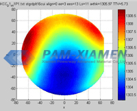
Semi-insulating GaAs Substrate
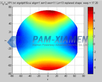
Semi-insulating GaAs Substrate
4. Application of Semi-insulatingg GaAs Substrate
Gallium arsenide material is one of the most important materials in the second generation of new compound semiconductors after silicon single crystals. Because of the excellent performance, high electron mobility and high photoelectric conversion efficiency, substrate of gallium arsenide is mainly used to fabricate integrated circuits with MESFET, HEMT and HBT structures, and the demand of semi-insulating GaAs substrate in the fields of radar, microwave and millimeter wave communications, ultra-high-speed computers and optical fiber communications is growing greatly. In addition, the wafers can be used for etch studies to determine etch rates of coatings on top of the wafer and how the etchants removing the coatings react with the GaAs wafer. Especially in the process of 5G commercialization, GaAs wafer will play an irreplaceable role.

For more information, please contact us email at victorchan@powerwaywafer.com and powerwaymaterial@gmail.com