The application fields of SiC wafers and GaN wafers are mainly divided into electronic power field, radio frequency field, optoelectronic field, and other fields. Among them, electronic power field and radio frequency field are the most important applications, and the advantages of using SiC material are obvious. These two areas have been introduced before, and semiconductor wafer fabrication techniques of GaN and SiC for optoelectronic devices will be discussed in the following part.
1. Semiconductor Wafer Fabrication in Terms of Luminescence
First of all, let’s start the semiconductor wafer fabrication process steps with luminescence. Semiconductors have a band gap, which can be used to emit laser light.
A practical laser has three elements: pump source, working substance, and resonant cavity. The pump source is like a power source, giving energy to the working material to emit laser light; the resonant cavity allows the lasers to be superimposed together to obtain higher power light; but the core is the working material—the energy level that can achieve population inversion structure.
It is necessary to be able to achieve population inversion, because laser is a type of stimulated radiation. There are other transition processes in semiconductor wafer processing steps. Only when the process of stimulated radiation is sufficient, can laser be displayed. Other processes include spontaneous emission, relaxation and other processes.
In order to achieve population inversion, the common energy level structure is a three-level structure. So the various processes between energy levels can be controlled.
For example, the realization of laser. The electron is pumped from the low energy level to the high energy level through the pump source; the electron is unstable at the high energy level, the electrons are stopped at the intermediate energy level by adding a relatively stable intermediate energy level. When there are enough electrons, the light will be very strong; Under the action of the resonant cavity, it is continuously amplified, which is the light amplified by stimulated radiation——laser.
2. Case Analysis for Semiconductor Wafer Fabrication on Optoelectronic Devices
In order to achieve a laser output of 1300nm (1.3um), a semiconductor laser was made. For semiconductor wafer manufacturing method, the required laser is output through 0.954eV InAs, and the energy change is converted into electric energy into GaAs, and then output laser, finally converted into InAs output laser.
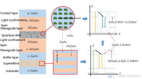
The whole GaAs semiconductor wafer manufacturing process (Figure above), the first is the underlying structure:
GaAs and AlGaAs are alternately arranged and thin enough to be a super lattice. The introduction of Al element allows the energy level of GaAs to be adjusted from 1.424eV to 2.168eV, and the corresponding high energy level can be obtained. GaAs is used as a middle energy level to output the pump laser. Under the action of electricity, electrons are continuously pumped to the high energy level of AlGaAs, and then jump down from the middle energy level of GaAs.
Then, it is the upper structure:
The output of the laser is derived from the preparation of the size of InAs to the nanometer level, which increases its energy gap from 0.354eV to 0.954eV (0.954eV=1240nm·eV/1300nm), making it a good intermediate energy level. The pump source is a GaAs laser obtained through the superlattice below. Under the action of the laser generated by GaAs, electrons are continuously pumped to the high energy level of GaAs, and then jump down from the middle energy level of InAs.
3. GaN and Luminescence
Lumi photons absorbed. In order to achieve this more conveniently, the energy level generally used has a structure with a direct band gap.
In fact, in addition to the above luminous GaAs and InP, the third-generation semiconductor material GaN also has a direct band gap. The data of common semiconductors is shown in the table below:
| Material | Bandgap | Band gap type | Breakdown field strength MV/cm |
Electron migration
rate |
Hole migration
rate |
Saturated electron drift rate 107cm/s |
Thermal conductivity w/(cm-K) |
Static dielectric constant | Hardness | |
| First Generation | Si | 1.12 | indirect | 0.3 | 1600 | 430 | 1 | 1.48 | 11.9 | 7 |
| Ge | 0.67 | indirect | 0.1 | 3900 | 1900 | 0.6 | 16.0 | 6.0 | ||
| Second Generation | GaAs | 1.42 | direct | 0.4 | 8500 | 400 | 1.3 | 0.55 | 13.1 | 4 |
| InP | 1.344 | direct | 0.45 | – | – | – | 0.68 | 12.5 | – | |
| Third Generation | GaN | 3.39 | direct | 2.6 | 1000 | 200 | 2.5 | 1.3 | 9 | – |
| AIN | 6.2 | direct | 1.2 | 300 | 14 | 1.4 | 2.85 | 9.14 | – | |
| Ga2O3 | 4.8 | direct | 8 | 300 | – | – | 0.3 | – | – | |
| 4H-SiC | 3.26 | indirect | 3 | 500 | 120 | 2.5 | 3.4 | 10.1 | 9.25 | |
| 6H-SiC | 2.86 | 1.2 | 260 | 50 | ||||||
| 3C-SiC | 2.2 | 1.2 | 900 | 320 | ||||||
| Last | Diamond | 5.5 | indirect | 20 | 2800 | 1300 | 2.7 | 22 | 5.7 | 10.0 |
- GaN is from PAM-XIAMEN.
GaN has a larger band gap than GaAs and InP. By adjusting this band gap, a wider range of light output can be obtained.
The band gap of GaAs is 1.42eV, which means that when the light below 873nm is generated. There will be a large absorption, and the light intensity will not work in semiconductor wafer fabrication systems.
The band gap of InP is 1.344eV, which means that when the light below 925nm is generated. There will be large absorption, and the light intensity will not work at this time.
The band gap of GaN is 3.4eV, which means that when the light below 364nm is generated. There will be a large absorption, and the light intensity will not work at this time.
It is the advantage of GaN that can produce visible light and ultraviolet light. The usage of the visible light in semiconductor wafer fabrication process: the blue LED is to add In and Al to the epitaxial GaN; lower wavelength light has greater energy and its professional uses, such as sterilization, marking, cutting, etc.
In order to prepare the GaN devices, SiC substrate has been selected again. The more details about why choose SiC substrate for a semiconductor wafer fabrication, please refer to The SiC Application in Radio Frequency Devices.

For more information, please contact us email at victorchan@powerwaywafer.com and powerwaymaterial@gmail.com.