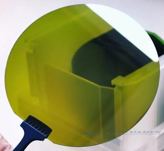
PAM-XIAMEN can offer SiC substrate and epitaxy wafer for fabricating IGBT devices. The emergence of the third-generation wide-bandgap semiconductor SiC wafer has shown stronger competitiveness in the fields of high voltage, high temperature, and high power. The n-IGBT (insulated gate bipolar transistor) is further developed by growing n– and p+ SiC thin film on the n-type SiC substrate as the drift layer and collector. And detailed structure of SiC IGBT wafer from PAM-XIAMEN is shown as follows:
1. Multi-Layer SiC Structure for N-Channel IGBT Fabrication
| Epi Layer | Thickness | Doping Concentration |
| n– drift layer | – | 2×1014cm-3 |
| n buffer layer | 3 um | – |
| p+ minority carrier injection layer | – | – |
| SiC substrate, n-type |
2. Opportunities of IGBT Devices based on SiC Substrate
IGBT is the core device of power conversion, which effectively contributes to carbon neutralization. In the field of clean energy power generation and utilization, IGBT is the core device of photovoltaic and wind power inverters, and is widely used in electric drive systems of new energy vehicles and charging piles. SiC IGBT module effectively reduces power consumption and helps achieve energy conservation and emission reduction. So the demand of SiC IGBT devices based on IGBT thin wafer technology will develop rapidly.
The demand for carbon neutrality is driving the rapid development of clean energy power generation and the rapid increase in the penetration of electric vehicles. On the consumption side, carbon neutrality puts forward stricter requirements for industrial electricity consumption, which further expands the popularization of energy-saving equipment such as frequency converters. As the core of power conversion, compare with Si IGBT, IGBT wafer fabrication on SiC material has great advantages in new energy vehicles. Therefore, the market space is huge.
3. Applications of Devices on SiC IGBT Wafer
At present, SiC epitaxial wafer is mainly used in main inverters, OBCs, DC/DCs, and compressors and IGBTs. Among them, epi IGBT is still the mainstream power devices used in the automotive field. SiC IGBT product portfolios in the automotive field are mainly based on bare chips, single tubes, power modules and components. The solutions based on thin wafer IGBT technology can cover energy vehicle applications, including main inverters, on-board chargers, PTC heaters, compressors, water pumps and oil pumps.
In the field of photovoltaic and wind power generation, IGBT silicon carbide is mainly used in inverters, so that the coarse electricity generated by photovoltaics or wind power can be processed by IGBTs into fine electricity that can be smoothly connected to the Internet.
In the field of industrial control and power supply, IGBTs based on 4H-SiC IGBT structure are widely used in inverters, servo machines, inverter welding machines and UPS power supplies.
In addition, in the field of home appliances, electronic Accessories fabricated on SiC IGBT epi wafer are used in white goods such as inverter air conditioners and inverter washing machines to help achieve energy saving and emission reduction.

For more information, please contact us email at victorchan@powerwaywafer.com and powerwaymaterial@gmail.com.