Due to the advantages of high thermal conductivity, high breakdown field strength, high saturation electron drift rate and high bonding energy, SiC material can meet the new requirements of modern electronic technology for high temperature, high frequency, high power, high voltage and radiation resistance, so it is regarded as one of the most promising materials in the field of semiconductor materials. PAM-XIAMEN can supply 4H-SiC seed crystal wafer, which is applied to 4 or 6 inch SiC crystal growth. Please refer to the following tables for specific parameters.
1. Specifications of SiC Seed Wafer
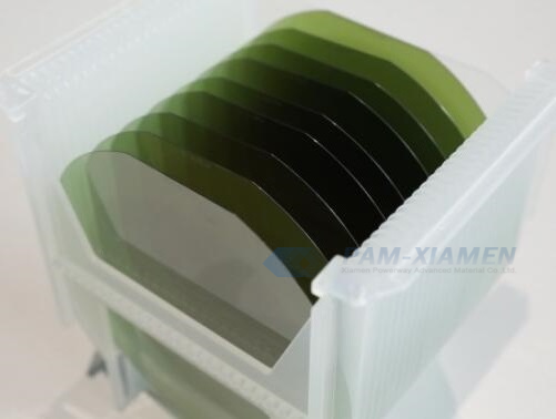
SiC Seed Wafer Application: growing SiC single crystals in 4 or 6 inch
1.1 4H-SiC Seed Crystal Wafer of 800um Thick
|
4H-SiC Seed Wafer Parameters |
||||
| No. | ltems | Production | Research | Unit |
| 1 | Crystal Parameters | |||
| 1.1 | Polytype | 4H | 4H | |
| 2 | Mechanical Parameters | |||
| 2.1 | Diameter | 104/150/153±0.5mm | 104/150/153±0.5mm | mm |
| 2.2 | Thickness | 800±50um | 800±50um | um |
| 2.3 | flat | None | None | um |
| 2.4 | TTV | ≤10um | ≤20um | um |
| 2.5 | LTV | ≤5um(5mm*5mm) | ≤10um(5mm*5mm) | um |
| 2.6 | Bow | -35um-35um | -45um~45um | um |
| 2.7 | Warp | ≤40um | ≤50um | um |
| 2.8 | Front (Si-face) Roughness | Ra≤0.2nm(5um*5um) | Ra≤0.2nm (5um*5um) | nm |
| 3 | Structure | |||
| 3.1 | Micropipe Density | ≤1ea/cm2 | ≤5ea/cm2 | ea/cm2 |
| 3.2 | Hexagonal void | None | None | |
| 3.3 | BPD | ≤2000 | NA | ea/cm2 |
| 3.4 | TSD | ≤500 | NA | ea/cm2 |
| 4 | Front Quality | |||
| 4.1 | Front | Si | Si | |
| 4.2 | Surface finish | Si-face CMP | Si-face CMP | |
| 4.3 | Scratches | ≤5pcs,≤2*Diameter (Cumulative Length) |
NA | ea/mm |
| 4.4 | Orange peelpits/stains/striationslcracks/contamination | None | None | mm |
| 4.5 | Edge chips/indents/fracture/hex plates | None | None | |
| 4.6 | Polytype areas | None | ≤30%(Cumulative area) | |
| 4.7 | Front laser marking | None | None | |
| 5 | Back Quality | |||
| 5.1 | Back finish | C-face CMP | C-face CMP | |
| 5.2 | Scratches | ≤2pcs,≤Diameter (Cumulative Length) |
NA | ea/mm |
| 5.3 | Back defects (edge chips/indents) | None | None | |
| 5.4 | Back roughness | Ra≤0.2nm (5um*5um) | Ra≤0.2nm (5um*5um) | nm |
| 5.5 | Back laser marking | 1mm (from top edge) | 1mm (from top edge) | |
| 6 | Edge | |||
| 6.1 | Edge | Chamfer | Chamfer | |
| 7 | Packaging | |||
| 7.1 | Packaging | Multi-wafer cassette | Multi-wafer cassette | |
1.2 4H-SiC Seed Wafer of 430~570um Thick
|
6inch SI 4H-SiC Seed Crytal Parameters |
||
| No. | Item | Parameter |
| 1 | Crystal Parameters | |
| 1.1 | Polytype | 4H |
| 2 | Mechanical Parameters | |
| 2.1 | Diameter | 150+0.1mm/-0.3mm |
| 2.2 | Thickness | 430um~570um |
| 2.3 | Surface Orientation | 1+0.4°/2±0.5° |
| 2.4 | Primary flat Orientation | {10-10}±0.5° |
| 2.5 | Primary flat length | 0-25mm or notch |
| 2.6 | Secondary flat | none |
| 2.7 | Resistivity | NA |
| 3 | Wafer Quality | |
| 3.1 | Micropipe density* | <1cm-2 |
| 3.2 | Micropipe dense area* | ≤3 places |
| 3.3 | Front scratches | none |
| 3.4 | Chips* | NA |
| 3.5 | Cracks* | NA |
| 3.6 | Pits* | none |
| 3.7 | Orange peel* | none |
| 3.8 | Contamination | none |
| 3.9 | Polytype Areas* | 0%(180° edge removal area opposite the secondary flat) |
| 3.10 | Polycrystalline* | none |
| 4 | Laser Marking | |
| 4.1 | Laser Marking | Above the primary flat on the Si-face |
| 5 | Edge | |
| 5.1 | Edge removal area | 3mm |
| Note:”*” data does not contain edge removal areas | ||
1.3 4Inch Seed Crystal of SiC
|
4Inch SiC Seed Crystal |
||
| Grade | Production | Research |
| Diameter | 100/105±0.5mm | |
| Thickness | 400±100um | 400±150um |
| Orientation | 4±1°(0±1°) | |
| Primary flat orientation | {1010}±0.5° | |
| Primary flat length | 32.5mm±2.0mm | |
| Secondary flat length | 18.0mm±2.0mm | |
| Edge removal area | 2mm | 3mm |
| TTV | ≤10um | ≤15um |
| Surface roughness | C: Ra≤1nm Si: Ra≤1nm |
|
| Polytype Areas* | None | |
| Polycrystalline* | None | |
| Hexagonal void* | None | |
| Micropipe Density* | ≤1cm-2 | ≤5cm-2 |
| Inclusion | ≤1% | ≤5% |
| Cracks | None | edge≤10mm, cental≤5mm |
| Chips | None | – |
| Macro scratches | None | – |
| Orange peel | None | – |
| Pits | None | – |
| Surface contamination | None | None |
| Note : “*” defects in the edge removal area are excluded. | ||
2. What Is A Seed Crystal?
A seed crystal is a small crystal with the same crystal orientation as the desired crystal, and is the seed for growing a single crystal. Using seed crystals with different crystal orientations as seeds, single crystals with different crystal orientations will be obtained. According to the use, there are Czochralski single crystal seed crystal, zone melting seed crystal, sapphire seed crystal and SiC seed crystal.
Therein, SiC wafer is used as a kind of seed crystal for SiC crystal growth, and the shape of SiC seed wafer is mainly in the form of thin film. It is reported that the application of seed crystal plays an important role in the growth of SiC crystal. The crystal form and surface properties of the SiC seed wafer greatly affect the growth type, defect structure and electrical properties of the SiC crystal.
Among them, the most important factor determining the single crystal polytype is the crystal orientation of the SiC seed wafer. The 6H-SiC ingot is grown on the SiC (0001, Si) face by the PVT method, even though the seed wafer is 4H-SiC (0001). On the contrary, 4H-SiC ingot is grown on SiC (0001, C) face by PVT method, which has nothing to do with the polytype of the seed crystal.
3. How to Make a Seed Crystal?
For making a seed crystal, firstly cut a bulk SiC single crystal into thin films, then grind, polish and etch the thin film to remove the pits and scratches produced by cutting. Grinding removes the layer of pits that cut the wafer surface, leaving thin, sparse scratches on the wafer surface. Polishing can remove the scratches produced during grinding, but not completely removed the grinding deterioration layer or the thin mechanical damage layer produced by polishing. Etching can not only reveal structural defects in the wafer, but also remove the surface mechanical damage layer produced during grinding and polishing. The etched wafer is used as a seed wafer, and the growth crystal can well replicate the structure of the seed crystal, and the crystal surface is smooth.
4. Why Use SiC Seed Substrate to Grow Single Crystal?
Most semiconductor single crystals can be grown from the molten state or solution, but the properties of SiC itself make it impossible to grow single crystals by these two methods.
At present, physical vapor transport (PVT) method is the most mature method among all the SiC growth techniques for growing SiC crystal. The method is to put the SiC seed substrate in a crucible containing SiC powder raw material, then the crucible is heated by an medium frequency induction or resistance furnace to make the temperature reach above 2000 ℃, and gas molecules containing Si and C are induced by temperature gradient between the raw material and the SiC seed, transferring to the seed wafer to grow SiC crystals. The significant difference between the PVT method and the early Lely method is that the PVT method introduces a seed crystal, which improves the controllability of the seed crystals crystallization growth process and is suitable for growing large-size SiC single crystals.

For more information, please contact us email at victorchan@powerwaywafer.com and powerwaymaterial@gmail.com.