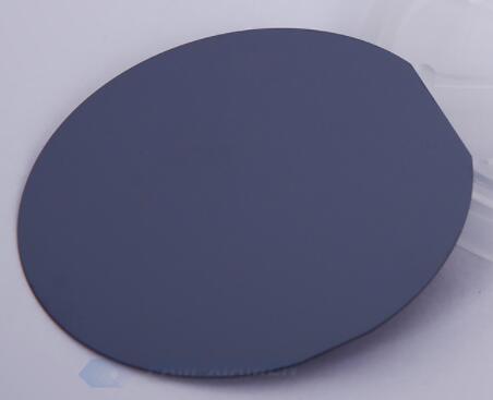
InP epitaxial wafers with solar cell structure that a p-InGaAs lattice matched to n-InP substrate can be provided by PAM-XIAMEN. Indium phosphide is one of the main group III-V compound semiconductors for manufacturing multi-compound solar cells. These multi-compound solar cells mainly include GaAs, InP, GaInP, AlGaInP, InGaAs, GaInNAs, CuInSe2, CuInGaSe, etc. and laminated solar cells composed of them. Following specifications are offered for reference, or you can provide us with custom solar cell structure design:

InGaAs/InP Solar Cell Structure
1. Bulk Heterojunction Solar Cell Structure
PAM170725-INGAAS
Structure 1. InP Epitaxial Structure for solar cell
| Layer No. | Composition | Concentration | Thickness | |
| 5 | Contact Layer | p++ InxGa1-xAs | 1E19 cm-3 | – |
| 4 | Window Layer and Front Surface Passivation | p+ AlxIn1-xAs | – | – |
| 3 | P Side of the PN Junction, Light Absorber | p+ InxGa1-xAs | – | – |
| 2 | Light Absorber | undoped InxGa1-xAs | – | – |
| 1 | Back Surface Field | n+ AlxIn1-xAs | – | 50nm |
| 0 | Substrate | n++ InP | highest possible doping | – |
Structure 2. Monocrystalline InP/InGaAs Solar Cell Structure
| Layer No. | Composition | Concentration | Thickness | |
| 3 | Contact Layer | p++ InxGa1-xAs | – | – |
| 2 | Window Layer | p+ AlxIn1-xAs | – | 50nm |
| 1 | P Side of the PN Junction, Light Absorber | p+ InxGa1-xAs | 1E18 cm-3 | – |
| 0 | Substrate | n++ InP | highest possible doping | – |
2. About Photovoltaic Solar Cell Structure Layer
A solar cell is a device that uses the photovoltaic effect to convert solar energy into direct current electrical energy through semiconductor materials (light energy is converted into electrical energy). Commercial solar cells mainly include crystalline silicon solar cells (including monocrystalline silicon and polycrystalline silicon) and semiconductor compound solar cells (mainly GaAs solar cell).
The working temperature of the high-temperature heat radiator is generally 1000°C~1500°C, so the solar cell band gap should be 0.4eV~0.7eV. Currently, more studies are carried out on thermal photovoltaic cells include Si, Ge, GaSb and InGaAs cells. Among them, InGaAs material is a typical ternary arsenide semiconductor material. Its band gap can be changed with the adjustment of its composition. The maximum adjustment can reach 1.424ev of gallium arsenide, and the minimum of indium arsenide can reach 0.356ev. Because of its wide adjustment range of the band gap, this can meet the band gap requirements required by thermal photovoltaic cells, so it is for thin film solar cell structure.
InGaAs materials often use InP as the substrate. The solar cell and crystal structure of InGaAs lattice-matched with the InP substrate has a band gap of 0.74eV. The InGaAs material with a band gap in the range of 0.5eV-0.6eV is comparable to InP wafer substrate, and the mismatch is between 1.0% and 1.4%. The stress buffer method can effectively reduce the density of misfit dislocations in the epitaxial layer, and at the same time control the dislocations in the buffer layer to avoid recombination centers caused by dislocations, increase the diffusion length of minority carriers, and greatly increase the short-circuit current density.
For more information, please contact us email at victorchan@powerwaywafer.com and powerwaymaterial@gmail.com.

