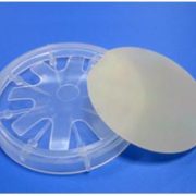

GaN Templates
- Beskrivning
Produktbeskrivning
GaN Template (gallium nitride template)
PAM-XIAMEN’s GaN Template consists of crystalline layers of gallium nitride (GaN), aluminum nitride (AlN), aluminum gallium nitride (AlGaN) and indium gallium nitride (InGaN), which are epilayer on sapphire and electronic grade for fabrication as MOS-based devices. PAM-XIAMEN’s Gallium Nitride Template Products enable 20-50% shorter epitaxy cycle times and higher quality epitaxial device layers, with better structural quality and higher thermal conductivity,which can improve devices in the cost, yield, and performance.
2″(50.8mm) GaN mallar Epitaxy on Sapphire Substrates
| Punkt | PAM-2inch-GaNT-N | PAM-2inch-GaNT-SI |
| ledningstyp | N-typ | Halvisolerande |
| dopningsmedel | Si doped or low doped | fe dopade |
| Storlek | 2 "(50 mm) diam. | |
| Tjocklek | 4um,20um,30um,50um,100um | 30um, 90um |
| Orientering | C-axel (0001) +/- 1 ° | |
| Resistivitet (300K) | <0.05Ω • cm | >1×10⁶Ω·cm |
| dislokation Densitet | <1x108cm-2 | |
| substrat struktur | GaN on Sapphire(0001) | |
| Ytfinish | Enkel eller Double Side Polerad, epi-ready | |
| användbar Area | ≥ 90% | |
2″ (50.8mm)GaN Templates Epitaxy on Sapphire Substrates
| Punkt | PAM-GANT-P | |
| ledningstyp | P-typ | |
| dopningsmedel | mg dopad | |
| Storlek | 2 "(50 mm) diam. | |
| Tjocklek | 5um, 20um, 30um, 50 um, 100um | |
| Orientering | C-axel (0001) +/- 1 ° | |
| Resistivitet (300K) | <1Ω • cm eller anpassade | |
| dopämneskoncentration | 1E17(cm-3) or custom | |
| substrat struktur | GaN on Sapphire(0001) | |
| Ytfinish | Enkel eller Double Side Polerad, epi-ready | |
| användbar Area | ≥ 90% | |
3″(76.2mm)GaN Templates Epitaxy on Sapphire Substrates
| Punkt | PAM-3inch-GaNT-N |
| ledningstyp | N-typ |
| dopningsmedel | Si doped |
| Uteslutning Zone: | 5mm från ytterdiametern |
| Tjocklek: | 20um,30um |
| Dislocation density | < 1x108cm-2 |
| Ytmotstånd (300K): | <0.05Ω • cm |
| Substrat: | sapphire |
| Orientation : | C-plane |
| Safir tjocklek: | 430um |
| Putsning: | Single sida Polerad, epi-ready, med atom steg. |
| Baksidesbeläggning: | (custom)high quality Titanium coating, thickness > 0.4 μm |
| Förpackning: | Individually packed under argon |
| Atmosphere vacuum sealed in class 100 clean room. |
3″(76.2mm)GaN Templates Epitaxy on Sapphire Substrates
| Punkt | PAM-3inch-GaNT-SI |
| ledningstyp | Halvisolerande |
| dopningsmedel | Fe Doped |
| Uteslutning Zone: | 5mm från ytterdiametern |
| Tjocklek: | 20um, (är 20um bäst) 30um, 90um |
| Dislocation density | < 1x108cm-2 |
| Ytmotstånd (300K): | >106 ohm.cm |
| Substrat: | sapphire |
| Orientation : | C-plane |
| Safir tjocklek: | 430um |
| Putsning: | Single sida Polerad, epi-ready, med atom steg. |
| Baksidesbeläggning: | (custom)high quality Titanium coating, thickness > 0.4 μm |
| Förpackning: | Individually packed under argon Atmosphere vacuum sealed in class 100 clean room. |
4″(100mm)GaN Templates Epitaxial on Sapphire Substrates
| Punkt | PAM-4inch-GaNT-N |
| ledningstyp | N-typ |
| dopningsmedel | lågdopad |
| Tjocklek: | 4um |
| Dislocation density | < 1x108cm-2 |
| Ytmotstånd (300K): | <0.05Ω • cm |
| Substrat: | sapphire |
| Orientation : | C-plane |
| Safir tjocklek: | – |
| Putsning: | Single sida Polerad, epi-ready, med atom steg. |
| Förpackning: | Individually packed under argon Atmosphere |
| vacuum sealed in class 100 clean room. |
2″ (50.8mm)AlGaN, InGaN, AlN Epitaxy on Sapphire Templates: custom
2”(50.8mm)AlN Epitaxy on Sapphire Templates
| Punkt | PAM-AlNT-SI |
| ledningstyp | semi-insulating |
| Diameter | Ф 50,8 mm ± 1 mm |
| Tjocklek: | 1000 nm +/- 10% |
| Substrat: | sapphire |
| Orientation : | C-axel (0001) +/- 1 ° |
| orientering Flat | Ett plan |
| XRD FWHM av (0002) | <200 bågsekunder. |
| Användbar Surface Area | ≥90% |
| Polishing: | Inget |
2”(50.8mm)InGaN Epitaxy on Sapphire Templates
| Punkt | PAM-INGAN |
| Conduction Type | – |
| Diameter | Ф 50.8mm ± 1mm |
| Tjocklek: | 100-200nm, custom |
| Substrat: | sapphire |
| Orientation : | C-axis(0001)+/-1O |
| dopningsmedel | |
| Dislocation Density | ~ 108 cm-2 |
| Useable Surface Area | ≥90% |
| Surface Finish | Single or Double Side Polished,epi-ready |
2”(50.8mm)AlGaN Epitaxy on Sapphire Templates
| Punkt | PAM-AlNT-SI |
| ledningstyp | semi-insulating |
| Diameter | Ф 50,8 mm ± 1 mm |
| Tjocklek: | 1000 nm +/- 10% |
| Substrat: | sapphire |
| Orientation : | C-planet |
| orientering Flat | Ett plan |
| XRD FWHM av (0002) | <200 bågsekunder. |
| Användbar Surface Area | ≥90% |
| Polishing: | Inget |
GaN Template on Sapphire& Silicon
2″(50.8mm)GaN on 4H or 6H SiC substrate
| 1)Undoped GaN buffer or AlN buffer are available; | ||||
| 2)n-type(Si doped or low doped), p-type or semi-insulating GaN epitaxial layers available; | ||||
| 3)vertical conductive structures on n-type SiC; | ||||
| 4)AlGaN – 20-60nm thick, (20%-30%Al), Si doped buffer; | ||||
| 5)GaN n-type layer on 330µm+/-25um thick 2” wafer. | ||||
| 6) Single or double side polished, epi-ready, Ra<0.5um | ||||
| 7)Typical value on XRD: | ||||
| Wafer ID | Substrate ID | XRD(102) | XRD(002) | Tjocklek |
| #2153 | X-70105033 (with AlN) | 298 | 167 | 679um |
| Single or double side polished, epi-ready, Ra<0.5um | ||||
6″ (150mm)n-GaN on double-side polished flat sapphire
| Target | remark | |
| Substrate diameter | 150 mm | +/- 0.15 mm |
| Substrate thickness | 1300 um or 1000um | +/- 25 um |
| c-plane (0001), offcut angle towards m-plane | 0.2 deg | +/- 0.1 deg |
| Single primary flat length | 47.5 mm | +/- 1 mm |
| Flat orientation | ett plan | +/- 0.2 deg |
| Si-doped n-GaN thickness | 4 um | +/- 5% |
| Si concentration in n-GaN | 5e18 cm-3 | ja |
| u-GaN thickness | 1 um | no this layer |
| XRD rocking curve (002) | < 250 arcsec | <300 arcsec |
| XRD rocking curve (102) | < 250 arcsec | <350 arcsec |
| Dislocation density | < 5e8 cm-2 | ja |
| Front side surface, AFM (5×5 um2) Ra | < 0.5 nm, Epi-ready | ja |
| Back side surfac\e | 0.6 – 1.2 um, fine ground | ja |
| Wafer bowing | < 100 um | no this data |
| n-GaN resistivity (300K) | < 0.01 ohm-cm2 | ja |
| Total thickness variation | < 25 um | <10um |
| Defect density | Macro defects (>100 um):< 1/wafer Micro defects (1-100 um):< 1/cm2 | Macro defects (>100 um):< 10/wafer Micro defects (1-100 um):< 10/cm2 |
| Lasermärkning | on the backside of the wafer flat | ja |
| Paket | packaged in a class 100 clean room environment, in cassettes of 25 pcs or single wafer containers, under nitrogen atmosphere, double sealed | ja |
| Edge exclusion | < 3 mm | ja |
| Useable surface area | > 90% | ja |
Hydride Vapour Phase Epitaxy (HVPE) process
GaN template on sapphire is grown by HVPE process and technology for the production of compound semiconductors such as GaN, AlN, and AlGaN. GaN templates are used in a wide applications: nanowire growth, solid state lighting, short wavelength optoelectronics and RF power device.
In the HVPE process, Group III nitrides (such as GaN, AlN) are formed by reacting hot gaseous metal chlorides (such as GaCl or AlCl) with ammonia gas (NH3). The metal chlorides are generated by passing hot HCl gas over the hot Group III metals. All reactions are done in a temperature controlled quartz furnace.
Anmärkning:
Den kinesiska regeringen har aviserat nya gränser för export av galliummaterial (som GaAs, GaN, Ga2O3, GaP, InGaAs och GaSb) och germaniummaterial som används för att tillverka halvledarchips. Från och med den 1 augusti 2023 är export av detta material endast tillåtet om vi får en licens från det kinesiska handelsministeriet. Hoppas på er förståelse och samarbete!
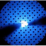
We will offer test reports, please see below an example:
AlGaN template structure report
More products:
GaN Thin Film on Sapphire (Al2O3) Template
Du kanske också gillar…
-
GaAs Epiwafer
PAM-XIAMEN tillverkar olika typer av epi wafer III-V kiseldopade n-typ halvledarmaterial baserade på Ga, Al, In, As och P odlade av MBE eller MOCVD. Vi levererar anpassade GaAs epiwafer-strukturer för att möta kundens specifikationer, kontakta oss för mer information.
-
Fristående GaN-substrat
PAM-XIAMEN har etablerat tillverkningstekniken för fristående (galliumnitrid) GaN substratskiva, som är för UHB-LED och LD. Vårt GaN-substrat har låg defektdensitet, odlat med HVPE-teknik (hydrid vapor phase epitaxi).
-
GaN baserad LED epitaxiell skiva
PAM-XIAMEN’s GaN(gallium nitride)-based LED epitaxial wafer is for ultra high brightness blue and green light emitting diodes (LED) and laser diodes (LD) application.
-
Test Wafer Övervaka Wafer Dummy Wafer
Som en dummy wafer tillverkare erbjuder PAM-XIAMEN silikon dummy wafer / test wafer / monitor wafer, som används i en produktionsenhet för att förbättra säkerheten i början av produktionsprocessen och används för leveranskontroll och utvärdering av processform. Eftersom dummy kiselwafers ofta används för experiment och test, är storlek och tjocklek därav viktiga faktorer i de flesta tillfällen. 100 mm, 150 mm, 200 mm eller 300 mm dummy wafer finns tillgänglig.
-
InAs wafer
PAM-XIAMEN erbjuder Compound Semiconductor InAs wafer - indium arsenid wafer som odlas av LEC (Liquid Encapsulated Czochralski) som epi-ready eller mekanisk kvalitet med n typ, p typ eller halvisolerande i olika orientering(111) eller (100). Dessutom har InAs enkristall hög elektronrörlighet och är ett idealiskt material för tillverkning av Hall-enheter.
-
Ge (germanium) enkristaller och Wafers
PAM-XIAMEN erbjuder 2”, 3”, 4” och 6” germaniumwafer, vilket är en förkortning för Ge wafer odlad av VGF/LEC. Lättdopad germaniumskiva av P- och N-typ kan också användas för experiment med Halleffekt. Vid rumstemperatur är kristallint germanium skört och har liten plasticitet. Germanium har halvledaregenskaper. Germanium med hög renhet dopas med trevärda grundämnen (såsom indium, gallium, bor) för att erhålla halvledare av P-typ germanium; och pentavalenta element (såsom antimon, arsenik och fosfor) dopas för att erhålla germaniumhalvledare av N-typ. Germanium har goda halvledaregenskaper, såsom hög elektronrörlighet och hög hålrörlighet. -
GaN HEMT epitaxiell skiva
Gallium Nitride (GaN) HEMTs (High Electron Mobility Transistors) are the next generation of RF power transistor technology. Thanks to GaN technology, PAM-XIAMEN now offer AlGaN/GaN HEMT Epi Wafer on sapphire or Silicon, and AlGaN/GaN on sapphire template.
-
SiC Wafer Substrat
Företaget har en komplett produktionslinje för SiC (kiselkarbid) wafersubstrat som integrerar kristalltillväxt, kristallbearbetning, waferbearbetning, polering, rengöring och testning. Nuförtiden levererar vi kommersiella 4H och 6H SiC-skivor med halvisolering och konduktivitet i on-axis eller off-axis, tillgängliga storlekar: 5x5mm2,10x10mm2, 2",3",4", 6" och 8", bryter igenom nyckelteknologier som t.ex. som undertryckande av defekter, bearbetning av frökristaller och snabb tillväxt, främjande av grundläggande forskning och utveckling relaterad till kiselkarbidepitaxi, enheter, etc.