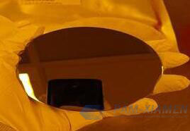
PAM-XIAMEN, a epi service supplier, offers service for processing laser wafer epitaxial growth on polished GaAs substrate and epi on bare substrates for power devices. In the PAM-XIAMEN’s wafer epitaxy foundry, GaAs epitaxy wafer with quantum well laser structure can be processed with the wavelength from the ultraviolet to the THz regime.

Laser epi wafers for the shortest wavelength are made on GaN-based material, and the epitaxial wafers with the longest wavelength are manufactured on quantum cascade laser design. We offer epi processing on GaAs as well as InP wafer, and then using MOVPE and MBE method for fabricating the lasers with discrete electron modes. When processing epitaxy on GaAs substrates by MBE, we strictly control the incident molecular or atmoic beam, which can grow a superlattice structure. When the epitaxial service for GaAs laser wafer processes with the MOVPE method, trimethylgallium or triethylgallium is used to interact with arsine to grow an epitaxial layer. The concentration, thickness and structure of the epi layer can be appropriately controlled.
Here is an example of GaAs epi structure produced by PAM-XIAMEN epi service:
808nm InGaAsP/GaAs MQW Laser structure
| Layer | Material | X | Y Strain tolerance | PL | Thickness | Type | Level | |
| (ppm) | (nm) | (um) | (cm-3) | |||||
| 8 | GaAs | 0.1 | P | >2.00E19 | ||||
| 7 | GaIn(x)P | 0.49 | +/-500 | 0.05 | P | |||
| 6 | [Al(x)Ga]In(y)P | 0.3 | 0.49 | +/-500r | 1 | P | ||
| 5 | GaIn(x)P | 0.49 | +/-500 | 0.5 | U/D | |||
| 4 | GaAs(x)P | 0.86 | +/-500 | 798 | 0.013 | U/D | ||
| 3 | GaIn(x)P | 0.49 | +/-500 | 0.5 | U/D | |||
| 2 | [Al(x)Ga]In(y)P | 0.3 | 0.49 | +/-500 | 1 | N | ||
| 1 | GaAs | 0.5 | N | |||||
| 0 | GaAs substrate | N | ||||||
The reaction of InGaAsP with oxygen is lower than that of AIGaAs, and the epitaxial growth resistivity for the device is lower than that of the aluminum device, but the thermal conductivity is higher. In addition, the surface recombination rate of InGaAsP is at least two orders of magnitude lower than that of AIGaAs, thereby reducing the temperature rise of the laser and improving the end surface resistance to catastrophic damage.
However, there is a disadvantage of InGaAsP/InGaP material. The waveguide layer is InGaAsP and the confinement layer is InGaP. Because the conduction band difference between the two is relatively small, it causes carrier leakage, which affects the higher threshold current density of InGaAsP/GaInP, which leads to the problem of the parameter characteristics of aluminum-free high-power lasers.
PAM-XIAMEN aims to develop more reliable semiconductor wafer and provide more advanced epi service for the customers all over the world. We have a professional epitaxy team with much experience to process your wafer, making sure the epi quality. The epi design can be offered by us, or you can send us the customized epitaxial structure design to process epitaxy in our epitaxial fab.

For more information, please contact us email at victorchan@powerwaywafer.com and powerwaymaterial@gmail.com.
