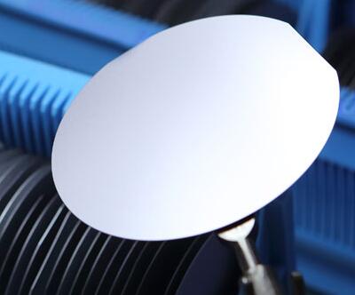
PAM XIAMEN offers Gallium Arsenide substrate with various sizes and low density. The GaAs wafer with the conductivity of N type, P type, or semi-insulating is for sale. In addition, you can offer your own wafer design to customize.
1. Main Parameters of Gallium Arsenide Substrate
| MAIN PARAMETERS FOR GAAS GALLIUM ARSENIDE ELECTRONIC GRADE CRYSTAL SUBSTRATES | |||||
| single crystal | Dopant | Conduction type | Carrier concentration cm-3 | Growth method | |
| Max size | |||||
| GaAs | None | SI | / | VGF | |
| Si | N | >5×10^17 | VGF | ||
| Cr | SI | / | VGF | ||
| Fe | N | ~2×10^18 | |||
| Zn | P | >5×10^17 | |||
| Sizes (mm) | 25×25×0.5mm, 10×10×0.5mm, 10×5×0.5mm, 5×5×0.5mm, 2 inch diameter | ||||
| Special size and orientation options are available upon request | |||||
| Surface Roughness | Surface roughness(Ra): <= 5A | ||||
| Polishing | Single or double side polished | ||||
2. Gallium Arsenide Wafer Substrate Standard
This standard applies to gallium arsenide single crystals and wafers used in optoelectronic devices and sensing elements. The standard is strictly obeyed by PAM-XIAMEN during the gallium arsenide substrate manufacturing process.
2.1 GaAs Wafer Electrical Performance
The electrical properties of gallium arsenide single crystal wafer should meet the requirements of Table 1.
Table 1 Electrical Performance of Gallium Arsenide Substrate
| Conductivity Type | Dopant | Carrier Concentration cm3 | Mobility cm3/(V. s) |
| N | Si | 8×10¹⁶~5×10¹⁸ | ≥1 100 |
| Te | 8×10¹⁶~5×10¹⁸ | ≥1 500 | |
| P | Zn | 1×10¹⁹~5×10¹⁹ | ≥50 |
2.2 GaAs Crystal Substrate Dislocation Density
Substrate of gallium arsenide is divided into 2 levels according to the dislocation density, which should meet the requirements of Table 2.
Table 2 Gallium Arsenide Dislocation Density
| Grades | Dislocation Density cm–2 |
| l | ≤5 000 |
| ll | ≤10 000 |
2.3 Gallium Arsenide Cutting Wafer Thickness
The thickness of the gallium arsenide substrate is 170um~650um, and the allowable deviation of the thickness is 15um~30um. The common thickness and allowable deviation of the GaAs substrate is 210um ± 20um, 280um ± 20um, 320um ± 20um, 350um ± 15um and 420um ± 15um.
2.4 GaAs Substrate Orientation Deviation
The deviation of the GaAs cutting wafer orientation and its allowable deviation should meet the requirements of Table 4. If there are special requirements, it shall be negotiated by the supplier and the buyer and indicated in the order form (or contract).
Table 4 Crystal Orientation Deviation and Allowable Deviation of GaAs Wafer Substrate
| Crystal Orientation Deviation | Allowable Deviation |
| (100) | ± 0.5° |
| (111) | ± 0.5° |
| (100) Deflection 1°~6° to (110) | ± 0.5° |
| (100) Deflection 1°~20° to (111) | ± 0.5° |
2.5 Reference Plane Orientation and Length of Gallium Arsenide Crystal Wafer
The orientation of the reference plane of the gallium arsenide single crystal substrate should meet the requirements of Table 5.
Table 5 Reference Plane Orientation of GaAs Thin Film
| Characteristic | The main reference plane is perpendicular to the V-groove | The main reference plane is perpendicular to the dovetail groove | ||
| Main reference plane | Secondary reference surface | Main reference plane | Secondary reference surface | |
| Orientation | (011) ±0.5° or projection direction on the wafer surface | Rotate 90°± 5° counterclockwise from the main reference surface | (011) ±0.5° or projection direction on the wafer surface | Rotate 90°±5° clockwise from the main reference surface |
| Features | Belongs to an As surface | Belongs to a Ga surface | Belongs to a Ga surface | Belongs to an As surface |
| Relationship with Groove | Perpendicular to the V-groove | Perpendicular to dovetail | Perpendicular to dovetail | Perpendicular to the V-groove |
2.6 Test Method for Gallium Arsenide Crystal and Wafer
The inspection of the surface quality of the gallium arsenide monocrystalline wafer substrate is carried out daily under good lighting;
The measurement of the diameter of the GaAs sheet shall be carried out with a vernier caliper with an graduation value not greater than 0.02mm;
The thickness of gallium arsenide thin film is measured with a micrometer with a graduation of 0.001 mm;
The measurement of the length of the reference surface of the gallium arsenide is carried out with a vernier caliper with an graduation value not greater than 0.02mm;
Inspection of the surface quality of gallium arsenide substrate is carried out daily under good lighting.

For more information, please contact us email at victorchan@powerwaywafer.com and powerwaymaterial@gmail.com.