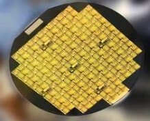
PAM XIAMEN offers 2 inch GaN (Gallium Nitride) HEMT Epitaxial Wafers on different substrates such as silicon substrate, sapphire substrate, silicon carbide (SiC) substrate. This GaN epitaxial wafer is for high-electron-mobility transistors (HEMT).
We sell directly from the factory, and therefore can offer the best prices on the market for high quality GaN HEMT epi-wafers. Customers from all over the world have trusted PAM XIAMEN Supplies as their preferred GaN epi wafer manufacture and gallium nitride producers.
1. Specifications of GaN Epi Wafer for HEMT
AlGaN/GaN HEMT on 2 in Conductive SiC Wafer (GaN/SiC)
AlGaN/GaN HEMT on 2 in Sapphire Wafer
AlGaN/GaN HEMT on 2 inch Semi-Insulating SiC Wafer (GaN/SiC)
AlGaN/GaN HEMT on 2 inch Si Wafer (GaN/Si)
In addition, PAM-XIAMEN can offer the GaN HEMT epi wafer as follows:
GaN on Si for Power, D-mode: The GaN HEMT Epitaxy Wafer on Si Substrate structure has an important property of high electron mobility due to the GaN/AlGaN. heterojunction structure.
GaN on Si for Power, E-mode: An enhanced HEMT device can be obtained by fabricating on GaN on Si wafer without applied voltage.
GaN on Si for RF: The GaN HEMT on Si wafer has There are obvious advantages in the high-power, high-frequency devices on HEMT epitaxial wafer of GaN on silicon.
GaN on Sapphire for Power: The GaN HEMT Epitaxy Wafer on sapphire is for power devices.
GaN on Sapphire for RF: This HEMT GaN epi-wafer is for fabricating radio frequency devices.
GaN on SiC for RF: HEMT stacks grown on semi-insulation SiC wafer for III-N material-growth and devices.
2. Industry Standards for 2” GaN based HEMT Epi Wafer
Gallium nitride provides a rugged and reliable technology for working under high voltage and high temperature, which makes GaN very targeted to open up many industrial, defense, medical and commercial applications.
2.1 Surface Quality of the Gallium Nitride Epiwafer
There should be no contamination on the surface of the epitaxial wafer, and the surface of the epitaxial wafer should be smooth and bright.
2.2 Gallium Nitride Wafer Dimensions
The external dimensions of the GaN epitaxial wafer should meet the requirements of Table 1.
Table 1 External Dimensions of GaN HEMT Epitaxial Wafer
| Parameters | Diameter | Flat |
| Specification | 50.8 mm ± 0.5 mm | 16.0 mm ± 1.0 mm |
Table 2 Electrical Properties of AlGaN / GaN HEMT Epitaxial Wafer
| No. | Properties | Parameters | Requirement | |
| Minimum | Maximum | |||
| HALL Test | Carrier Mobility | 1800 cm2/V-s | / | |
| 2DEG Areal Density | 6*1012 cm-2 | / | ||
| Square Resistance | / | 500 Ω/□ | ||
| 2 | XRD Rocking Curve Half-height Width | 002 | / | 250 s |
| 102 | / | 250 s | ||
| 3 | AFM Test | Roughness | / | 0.5nm |
2.3 Thickness of GaN Epitaxial Layer and Standard Deviation of Thickness
The thickness of the epitaxial layer is measured using the PL mapping test system:
The diameter of the test displayable area: ≤50mm;
Test resolution: 0.1mm~5mm;
Test scan speed: 1~30pts/s;
Laser wavelength: 266nm;
Laser power: 4.1mW~22.24mW;
Laser power density: 52W/cm2~283.5W/cm2;
Slit width: 0.01mm~2mm.
The parameters are complying with electrical properties in the Table 2.
2.4 Hall Test for GaN HEMT Epitaxial Wafer
Hall test measures the carrier mobility, 2DEG areal density and square resistance of the gallium nitride wafer for HEMT:
Magnetic field strength: 0.45T permanent magnet;
Resistivity range: 1u ohm*cm~10M ohm*cm;
Resistance range: 0.1m ohms~10 G ohms;
Carrier concentration: 1E+7cm-3~1E+21cm-3
Mobility: 1E-2cm2/(volt*sec)~1E+7cm2/(volt*sec);
The test result is accord with the requirement in Table 2.
2.5 XRD TEST for GaN Epitaxial Wafer with HEMT Stacks
Double crystal diffraction is used to measure the 002-face and 102-face rocking curves of the bulk material:
The half-height wide scan range is -35°~170°;
Scanning speed 0.006°/min~120°/min;
Minimum step angle 0.0001°;
Measurement accuracy ≤0.0002°;
2ѳ-angle repeatability 0.0005°;
Angular positioning speed 1500°/min(20).
The result of XRD rocking curve half-height width for GaN epitaxial wafer meets the requirement in the table 2.
3. GaN / AIGaN HEMT Epi Wafer Development
In GaN epitaxial wafer market, the early development of GaN/AIGaN HEMT technology is mainly concentrated in three main areas, including improving the quality of epitaxial layer materials, selecting the best substrate material, and developing the development unit process. In the field of optoelectronics, many developments of gallium nitride and aluminum gallium nitride heteroepitaxial are based on the early metal organic chemical vapor deposition method. However, for multi-gallium nitride electronic devices, MBE and MOCVD growth methods are considered feasible. Due to the availability of sapphire, most advanced methods of GaN HEMT epitaxial growth have been realized on sapphire. However, commercial HEMT devices on gallium nitride fabrication use low-cost Si substrates or 4H and 6H SiC substrate with superior high-power performance and superior thermal conductivity. The technological level of power devices on SiC substrates can reach 500W at 2.9GHz, 800W and 3.5GHz.
AlGaN/GaN HEMTs have a high breakdown voltage, allowing a large leakage voltage to be used, which leads to a large output impedance of the RF power inverter and leads to easy matching and low-loss matching circuits. The high surface charge leads to a large current density, the reduction of the transistor area leads to a large power density on the gate surface, and a high saturation drift speed leads to a high saturation current density and gate power density, which in turn leads to a decrease the unit capacitance of the output power. Low output capacitance and drain-source impedance make HEMT on GaN epitaxial wafer very suitable for switching amplifiers.

For more information, please contact us email at victorchan@powerwaywafer.com and powerwaymaterial@gmail.com.