We are one of the world’s leading glass wafer suppliers, provide thin & ultra-thin glass wafers and substrates which are made of different materials, such as Borofloat, Fused Silica & Quartz, BK7, Soda Lime etc for MEMS, fiber optic AWG, LCD panels och OLED substrates application. These wafers are all SEMI Standards including dimensional, flat and notch specifications, also we offer custom specifications designed to your unique needs including alignment marks, holes, pockets, edge profile, thickness, flatness, surface quality, cleanliness or any other details critical to your application, including semiconductor, medical science, communications, lasers, infrared, electronics, measuring instruments, military, and aerospace.
1. Specification of Glass Wafer
| Parameter | Measurement |
| Diameter | 2 ", 4", 6 ", 8", 10 " |
| Dimensional Tolerance | ±0.02μm |
| Tjocklek | 0.12mm, 0.13mm, 0.2mm, 0.25mm, 0.45mm |
| Thickness Tolerance | ± 10 ^ m |
| Thickness Variation (TTV) | < 0.01mm |
| Flatness | 1/10 Wave/Inch |
| Surface Roughness (RMS) | <1.5nm |
| Scratch and Dig | May 2nd |
| Particle Size | <5μm |
| Bow/Warp | <10 ^ m |
| For the customized dimension, please contact us | |
2. Glass Wafer Process
Wafer Cutting: Tom skiva är redo genom att tjocka lakan vattensprutas och block sås med tråd
Markkanten: skivkanten är cylindrisk jordad på kantslipstationen.
Wafer Lapping: skivan släpps till bestämd tjocklek.
Wafer Polering: Polering av skivan ger den speglade, super-plana ytan som krävs för tillverkningen.
Rengöring av rån: det är avlägsnande av kemiska föroreningar och partiklar utan att ändra eller skada skivytan eller substratet på flera rengöringslinjer.
Wafer Inspection: inspektera till olika kvalitetsnivåer under lämpligt ljusförhållande i klass 100 renrum.
Wafer-förpackning: Alla skivor är förpackade i de enda skivbehållarna.
3. Överföring av glasskivor
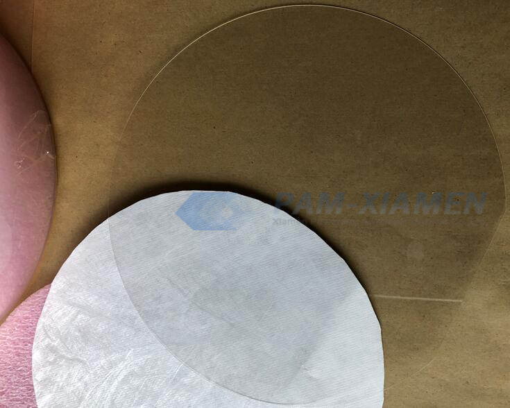
Glass Wafer
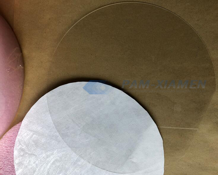
Överföring av glasskivan
4. Scratch/Dig Inspection Standard for Glass Wafer
We inspect the glasses for scratches by strong light (Multi-angle parallel light source) in a dark room.
Inspection Purpose: To determine whether there are fine scratches, foreign bodies, microbubbles on the glass surface.
Inspection Content: Inspect for fine scratch on glass surface
Reference Light Source: Multi-angle parallel light source
Analysis: The inspection for fine scratch, foreign matter on glass surface.
The glass is a highly reflective object, and the multi-angle parallel light source can illuminate the fine scratches clearly, and very uniform.
Scratch/Dig: 60/40 means:
60: max allowable scratch width (0.06mm width)
40: max allowable dig diameter (0.4mm diameter)
More about the scratch or dig number, please refer to the table below:
| Scratch Number | Maximum Allowable Scratch Width (mm) |
Dig Number | Maximum Allowable Dig or Bubble Diameter (mm) |
|
| 120 | 0.12 | 120 | 1.2 | |
| 80 | 0.08 | 80 | 0.8 | |
| 60 | 0.06 | 60 | 0.6 | |
| 50 | 0.05 | 50 | 0.5 | |
| 40 | 0.04 | 40 | 0.4 | |
| 30 | 0.03 | 30 | 0.3 | |
| 20 | 0.02 | 20 | 0.2 | |
| Purpose: glass surface quality on optical components Definitions: Procedure: |
||||
För mer information, vänligen kontakta oss maila påvictorchan@powerwaywafer.com och powerwaymaterial@gmail.com.