Silicon carbide has a variety of crystal types, but the silicon crystal structure the market needed is mainly 4H-SiC. So the silicon carbide crystal growth in crystal types is a defect. To a certain extent, it can be distinguished by the naked eye. A more accurate measurement method for testing the silicon carbide crystal distribution is Raman spectroscopy: Raman spectroscopy has characteristics for crystals, and the peak positions of the light emitted by different crystals are different.
1. What is Raman Spectroscopy?
1928 upptäckte den indiska forskaren Raman Ramanspridning i experimentet med att studera spridningsspektret för flytande bensen. Ramans spridningsspektroskopi, i enkla termer, är att använda en ljusstråle som infaller på ett ämne, frekvensen för det infallande ljuset är v och frekvensen för det resulterande spridda ljuset kommer att vara v, v + Av1, v-Av1, v + Av2, v-Av2, och så vidare. Dessa Av1, Av2, etc. Av har egenskaper. Med andra ord har varje substans en viss skillnad (topposition, toppintensitet), som kallas Raman-skift (det emitterade ljuset minus det infallande ljuset).
Till exempel är Ramans spektrum av 4H-SiC:
| Raman-skift (cm-1) | E2 tvärgående akustisk våg | E2 tvärgående akustisk våg | A1 tvärgående akustisk våg | E2 tvärgående akustisk våg | A1 tvärgående akustisk våg | A1 längsgående akustisk våg | LOPC | LOPC |
| 4H-SiC | 194.958 | 204.034 | 610.031 | 776.489 | 796.861 | 963.106 | 964.769 | 994.643 |
The table above shown here is the Raman shift. During the silicon carbide crystal distribution measurement, the computer will help to calculate it and process it as a Raman shift spectrum.
2. How to Test the Silicon Carbide Crystal Distrubution?
Typiska testförhållanden är: med 532nm-lasern från Ar + -laserna i LabRAM HR Raman-spektrometern, infaller den vertikalt, exciteringseffekten är 200mW och sättet att samla spridd ljus är bakspridningsläget. Det infallande ljuset med olika våglängder har olika penetrationsdjup. Generellt är 266nm-lasern 0,2um, 325nm-lasern 2um och 514nm-lasern är 30um, vilket innebär att ultraviolett ljus endast kan användas för att mäta tunna prover.
Because the silicon carbide wafer has different positions, multiple measurements will be taken to obtain the silicon carbide crystal distribution:
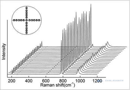
The data has three indicators: the position of the peak, the height of the peak (light intensity), and the width of the peak. Only when the peak position is completely matched, can it be den kvalificerade 4H-SiC. Som med XRD, närhelst det finns andra toppar, är de ämnen i andra faser, vilket är en defekt.
The difference in the position of the peak is due to the difference in the energy of the phonons brought about by the different silicon carbide crystal lattices, that is, the different frequencies. Each phonon has its corresponding energy level. The virtual energy level theory can be used to explain Raman (non-linear process):
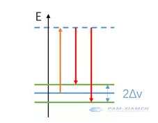
Partikeln absorberar infallande ljus till den virtuella energinivån (orange) och övergår sedan tillbaka till en vibrationsenerginivå (röd) som skiljer sig från den ursprungliga energinivån. Eftersom den övre energinivån är en virtuell energinivå kan frekvensen för det infallande ljuset varieras så länge det inte strider mot den ursprungliga verkliga energinivån.
Det är värt att notera att LOPC-läget (964,769 cm-1) kan användas för att analysera bärarkoncentrationen:
n = 1.25 * 1017cm-2 *(964.769cm-1-VLOPC measurement)
As the carrier concentration increases, the interaction between atoms and the lattice increases, which makes the Raman peak blue shift (smaller), the intensity decreases, and the width increases. This method is not as accurate as other methods and can only be used as an aid to analyze the silicon carbide crystal distribution.
3. Why not Use XRD to Measure Silicon Carbide Crystal Distribution?
X-rays are optical radiation generated by the transition of electrons in the inner layer of atoms under the bombardment of high-speed moving electrons, including continuous X-rays and characteristic X-rays. Silicon carbide single crystal can be used as X-ray gratings, and the coherent scattering produced by these large numbers of particles (atoms, ions, or molecules) will cause light interference, increasing or decreasing the intensity of scattered X-rays. Due to the superposition of scattered waves from a large number of particles, the beams that interfere with each other to produce the highest intensity are called X-ray diffraction lines.
För att uppfylla diffraktionsvillkoren kan Bragg-formeln tillämpas: 2dsinθ = nλ.
Den infallande strålen får varje spridare att utstråla en liten del av sin intensitet som en sfärisk våg. Om spridarna är ordnade symmetriskt med intervallet d kommer dessa sfäriska vågor endast att synkroniseras i den riktning där deras banlängdsskillnad 2dsinθ är lika med ett heltal multipel av våglängden λ. I detta fall avböjs en del av den infallande strålen med en vinkel på 2 of, vilket ger reflektionspunkter i diffraktionsmönstret.
Use X-rays of known wavelengths to measure the θ angle to calculate the interplanar spacing d, which is used for X-ray structure analysis; the other is to use a silicon carbide seed crystal with a known d to measure the θ angle to calculate the characteristic X-ray wavelength, and then the elements contained in the sample can be found in the existing data.
The measurement formula is 2dSinθ=λ. While the d value among the cubic silicon carbide crystal is close, and the characteristic is not obvious enough, the accurate silicon carbide crystal distribution cannot be precisely determined. For these reasons, it is not suitable to use the XRD to measure the distribution of silicon carbide crystals.

För mer information, kontakta oss via e-post på victorchan@powerwaywafer.com och powerwaymaterial@gmail.com.