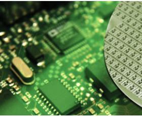


SiC Epitaxy
- Beskrivning
Produktbeskrivning
SiC Epitaxi
PAM-XIAMEN provide custom thin film (silicon carbide) SiC epitaxy on 6H or 4H substrates for the development of silicon carbide devices. SiC epi wafer is mainly used for the fabrication of 600V~3300V power devices, including SBD, JBS, PIN, MOSFET, JFET, BJT, GTO, IGBT, etc. With a silicon carbide wafer as a substrate, a chemical vapor deposition (CVD) method is usually used to deposit a layer of single crystal on the wafer to form an epitaxial wafer. Among them, SiC epitaxy are prepared by growing silicon carbide epitaxial layers on conductive silicon carbide substrates, which can be further fabricated into power devices.
1. specifikation av SiC epitaxi:
| Objekt | Specifikation | Typiskt värde |
| Poly-typ | 4H | — |
| Off-orientering mot | 4 deg-off | — |
| <11 2_ 0> | ||
| Ledningsförmåga | n-typ | — |
| dopningsmedel | Kväve | — |
| bärarkoncentration | 5E15-2E18 cm-3 | — |
| Tolerans | ± 25% | ± 15% |
| Enhetlighet | 2 ”(50,8 mm) <10% | 7% |
| 3 "(76,2 mm) <20% | 10% | |
| 4 ”(100 mm) <20% | 15% | |
| Tjocklek | 5-15 μm | — |
| Tolerans | ± 10% | ± 5% |
| Enhetlighet | 2 ”<5% | 2% |
| 3 ”<7% | 3% | |
| 4 ”<10% | 5% | |
| Stora punktfel | 2 ”<30 | 2 ”<15 |
| 3 ”<60 | 3 ”<30 | |
| 4 ”<90 | 4 ”<45 | |
| Epi-defekter | ≤20 cm-2 | ≤10 cm-2 |
| Step Bunching | ≤2,0 nm (Rq) | ≤1,0 nm (Rq) |
| (Grovhet) |
2 mm kantuteslutning för 50,8 och 76,2 mm, 3 mm kantuteslutning för 100,0 mm Anmärkningar:
• Genomsnitt av alla mätpunkter för tjocklek och bärarkoncentration (se s. 5)
• Epi-skikt av N-typ <20 mikron föregås av n-typ, 1E18, 0,5 mikron buffertlager
• Inte alla dopningstätheter finns i alla tjocklekar
• Enhet: standardavvikelse (σ) / genomsnitt
• Eventuella speciella krav på epi-parametern är på begäran
2. Introduction of SiC Epitaxy
Why do We Need Silicon Carbide Epitaxial Wafer? Because different from the traditional silicon power device manufacturing process, silicon carbide power devices cannot be directly fabricated on silicon carbide single crystal materials. High-quality epitaxial materials must be grown on conductive single crystal substrates, and various devices manufactured on the SiC epitaxial wafer.
The main epitaxial technology for SiC epitaxy growth is chemical vapor deposition (CVD), which realizes a certain thickness and doped silicon carbide epitaxial material through the growth of SiC epitaxy reactor step flow. With the improvement of silicon carbide power device manufacturing requirements and withstand voltage levels, SiC epi wafer continues to develop in the direction of low defects and thick epitaxy.
In recent years, the quality of thin silicon carbide epitaxial materials (<20 μm) has been continuously improved. The microtubule defects in the epitaxial materials have been eliminated. However, the SiC epitaxy defects, such as drop, triangle, carrot, screw dislocation, basal plane dislocation, deep-level defects, etc., become the main factor affecting device performance. With the advancement of SiC epitaxy process, the thickness of the epitaxial layer has developed from a few μm and tens of μm in the past to the current tens of μm and hundreds of μm. Thanks to the advantages of SiC over Si, the SiC epitaxy market is growing rapidly.
Since silicon carbide devices must be fabricated on epitaxial materials, basically all silicon carbide single crystal materials will be used as SiC epitaxial film to grow epitaxial materials. The technology of silicon carbide epitaxial materials has developed rapidly internationally, with the highest epitaxial thickness reaching more than 250 μm. Among them, the epitaxy technology of 20 μm and below has a high maturity. The surface defect density has been reduced to less than 1/cm2, and the dislocation density has been reduced from 105/cm2 to 103/cm2. The dislocation conversion rate of base plane is close to 100%, which has basically met the requirements of epitaxial materials for large-scale production of silicon carbide devices.
In recent years, the international 30 μm~50 μm epitaxial material technology has also matured rapidly, but due to the limitation of SiC epi market demand, the progress of industrialization has been slow. At present, industrialization company can offer silicon carbide epitaxial materials in batches, include Cree SiC epitaxy, PAM-XIAMEN SiC epitaxy, Dow Corning SiC epitaxy etc..
3.Test Methods
Nr 1. Bärarkoncentration: Nettodoping bestäms som ett medelvärde över det ovanstående med användning av Hg-sond CV.
Nr 2. Tjocklek: Tjockleken bestäms som ett medelvärde över skivan med FTIR.
Nr 3 Storleksdefekter: Mikroskopisk inspektion utförd vid 100X, på ett Olympus optiskt mikroskop eller jämförbart.
Nr 4. Epi Defects Inspection eller defekt karta utförd under KLA-Tencor Candela CS20 Optical Surface Analyzer eller SICA.
Nr 5. Steggruppning: Steggruppning och grovhet skannas av AFM (atomkraftmikroskop) på ett område på 10 μm x 10 μm
3-1:Large Point Defects Descriptions
Defekter som uppvisar en tydlig form för det oassisterade ögat och är> 50 mikron över. Dessa funktioner inkluderar spikar, vidhäftande partiklar, flisor och fräsar. Stora spetsdefekter med mindre än 3 mm mellanrum räknas som en defekt.
3-2:Epitaxy Defect Descriptions
SiC epitaxy defects include 3C inclusions, comet tails, carrots, particles, silicon droplets and downfall.
4. Application of SiC epitaxial wafer
Effektfaktorkorrigering (PFC)
Omvandlare för PV-omvandlare och UPS (oavbruten strömförsörjning)
Motordrivenheter
Korrigering av utdata
Hybrid- eller elfordon
SiC Schottky-diod med 600V, 650V, 1200V, 1700V, 3300V är tillgänglig.
Se nedan detaljerad ansökan per fält:
| Fält | Radiofrekvens (RF) | Power-enhet | LED |
| Material | SiLDMOS | Si | GaN / Al2O3 |
| GaAs | GaN / Si | GaN / Si | |
| GaN / SiC | SiC / SiC | GaN / SiC | |
| GaN / Si | Ga203 | / | |
| anordning | SiC-baserad GaN HEMT | SiC-baserad MOSFET SiC-baserad BJT SiC-baserad IGBT SiC-baserad SBD |
/ |
| Ansökan | Radar, 5G | Elektriska fordon | Halvljusbelysning |
5. Mechanical wafers with Epi layes: are available, such as for process monitoring, which require wafers with low bow and warpage.
Intrinsic SiC Epilayer on Silicon carbide substrate
Why do We Need Silicon Carbide Epitaxial Wafer?
SiC MOSFET Structure Homoepitaxial on SiC substrate
Du kan också gilla ...
-
SiC Wafer Reclaim
PAM-XIAMEN kan erbjuda följande SiC Reclaim wafer tjänster.
-
Ge (germanium) enkristaller och Wafers
PAM-XIAMEN erbjuder 2”, 3”, 4” och 6” germaniumwafer, vilket är en förkortning för Ge wafer odlad av VGF/LEC. Lättdopad germaniumskiva av P- och N-typ kan också användas för experiment med Halleffekt. Vid rumstemperatur är kristallint germanium skört och har liten plasticitet. Germanium har halvledaregenskaper. Germanium med hög renhet dopas med trevärda grundämnen (såsom indium, gallium, bor) för att erhålla halvledare av P-typ germanium; och pentavalenta element (såsom antimon, arsenik och fosfor) dopas för att erhålla germaniumhalvledare av N-typ. Germanium har goda halvledaregenskaper, såsom hög elektronrörlighet och hög hålrörlighet. -
GaAs Epiwafer
PAM-XIAMEN tillverkar olika typer av epi wafer III-V kiseldopade n-typ halvledarmaterial baserade på Ga, Al, In, As och P odlade av MBE eller MOCVD. Vi levererar anpassade GaAs epiwafer-strukturer för att möta kundens specifikationer, kontakta oss för mer information.
-
Cz Mono-kristallint kisel
PAM-XIAMEN, en monokristallin kiseltillverkare i bulk, kan erbjuda <100>, <110> och <111> monokristallina kiselskivor med N&P-dopningsmedel i 76,2~200 mm, som odlas med CZ-metoden. Czochralski-metoden är en kristalltillväxtmetod, kallad CZ-metoden. Den är integrerad i ett värmesystem med raka rör, värms upp av grafitmotstånd, smälter polykiseln som finns i en högrent kvartsdegel och för sedan in frökristallen i smältans yta för svetsning. Därefter sänks den roterande frökristallen och smälts. Kroppen infiltreras och berörs, höjs gradvis och avslutas eller dras genom stegen necking, necking, skuldra, kontroll med samma diameter och finish.
-
SiC Wafer Substrate
Företaget har en komplett produktionslinje för SiC (kiselkarbid) wafersubstrat som integrerar kristalltillväxt, kristallbearbetning, waferbearbetning, polering, rengöring och testning. Nuförtiden levererar vi kommersiella 4H och 6H SiC-skivor med halvisolering och konduktivitet i on-axis eller off-axis, tillgängliga storlekar: 5x5mm2,10x10mm2, 2",3",4", 6" och 8", bryter igenom nyckelteknologier som t.ex. som undertryckande av defekter, bearbetning av frökristaller och snabb tillväxt, främjande av grundläggande forskning och utveckling relaterad till kiselkarbidepitaxi, enheter, etc.
-
SIC Application
På grund av att SiC-fysiska och elektroniska egenskaper, kiselkarbid baserad enhet är väl lämpade för kort våglängd optoelektroniska, hög temperatur, strålningsresistenta, och hög effekt / högfrekventa elektroniska enheter, jämfört med Si och GaAs-enhet -
InP rån
PAM-XIAMEN erbjuder VGF InP(Indium Phosphide) wafer med prime eller test grade inklusive low dope, N-typ eller halvisolerande. InP-skivans rörlighet är olika i olika typer, lågdopad en>=3000cm2/Vs, N-typ>1000 eller 2000cm2V.s(beror på olika dopningskoncentrationer), P-typ: 60+/-10 eller 80+/-10cm2 /Vs(beror på olika Zn-dopningskoncentration), och halvförolämpande en>2000cm2/Vs, EPD för indiumfosfid är normalt under 500/cm2.
-
Fristående GaN-substrat
PAM-XIAMEN har etablerat den tillverkningsteknik för fristående (galliumnitrid) GaN substratskivan, som är för UHB-LED och LD. Vuxit med hydrid ångfasepitaxi (HVPE) teknik, har Vår GaN-substrat med låg defektdensitet.