We are an expert of semiconductor wafers in semiconductor industry, and we offer technology support and wafers selling for thousands of univerisities and industrial customers by our decades experience, including Cornell University, Stanford Univeristy,Peking University, Shandong Univerity, university of south carolina,Caltech Faraon lab (USA),University of California, Irvine (USA),Singapore MIT Alliance for Research and Technology Centre (SMART),West Virginia University,Purdue Univerity, University of California, Los Angeles,King Abdullah University of Science & Technology,Massachusetts Institute of Technology,University of Houston,University of Wisconsin,University of Science and Technology of China etc.
And now we show one article example as follows, who bought our wafers or service:
Article title:
The role of carbon and SiO2 in solid-state sintering of SiC
Published by:
Eran Gross;Dana Benes Dahan;Wayne D. Kaplan.
Department of Materials Science and Engineering, Technion—Israel Institute of Technology, Haifa 32000, Israel.
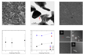
Picture of SiC:
Abstract
The role of carbon in reducing SiO2 during solid-state sintering of SiC was directly shown using a model experiment, where transmission electron microscopy was used to follow oxidation and reduction of the surface of SiC single crystals. These results corroborated the microstructural characterization of pressureless sintered polycrystalline SiC, undoped or doped with carbon (3 wt.%) and boron (0.5 wt.%). While samples doped with carbon and boron reached a density of 96% after 4 h of sintering at 2100 °C, undoped samples did not sinter, and the microstructure was characterized by particle coarsening and a film of SiO2. The lack of densification for undoped samples is explained by the low surface energy of SiO2 compared to the grain boundary energy of SiC, which reduces the driving force for densification.
Subject(s): SiC ; Sintering ; Dopants, Surface energy ; TEM ; Carbon.
Article abstract for Using Wafer from Xiamen Powerway Advanced Material Co. Ltd. (PAM-XIAMEN) or Powerway Wafer Co.,Limited
“… 2.2. Model experiments: Oxidation/reduction. 6H SiC single crystals (Xiamen Powerway
Advanced Material, N-doped) were used in the oxidation-reduction experiments.
Transmission electron microscopy (TEM) plan-view samples …”
Source:
https://www.sciencedirect.com/science/article/abs/pii/S0955221915000023
About Xiamen Powerway Advanced Material Co., Ltd
PAM-XIAMEN offers semiconductor silicon carbide wafers,6H SiC and 4H SiC wafer in different quality grades for researcher and industry manufacturers. We has developed SiC crystal growth technology and SiC wafer processing technology. We provide custom thin film (silicon carbide)SiC epitaxy on 6H or 4H substrates for the development of silicon carbide devices. SiC epi wafer is mainly used for Schottky diodes, metal-oxide semiconductor field-effect transistors, junction field effect.
PAM-XIAMEN also offer GaAs/InP and GaN material from wafer substrate to epitaxial growth.
Powerway Wafer Co.,Limited is a sub company of Xiamen Powerway Advanced Material Co., Ltd specialize in dealing with overseas orders.
Are You Looking for an Semiconductor wafer?
PAM-XIAMEN is your go-to place for everything wafers, including SiC/GaN/GaAs/InP wafer with wafer or epitaxial wafer, as we have been doing it for almost 30 years! Enquire us today to learn more about the wafers that we offer and how we can help you with your next project. Our group team is looking forward to providing both quality products and excellent service for you! For more information, please visit our website:www.powerwaywafer.com, send us email at tech@powerwaywafer.com or powerwaymaterial@gmail.com.