Thermodynamics and kinetic theory of nucleation and the evolution of liquid precipitates in gallium arsenide wafer
We study nucleation and evolution of liquid droplets in semi-insulating solid gallium arsenide (GaAs). For a realistic modelling, the crucial issue of a combined thermodynamic and kinetic treatment is the coupling of diffusion, chemical reactions and interface motion with local inhomogeneous mechanical stress fields in the solid matrix. In this note we present a hierarchy of models on various space scales. With more detail we discuss a kinetic model for the Becker–Döring regime and a thermodynamic model to describe diffusion in the vicinity of a single droplet.
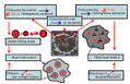
Fig. 1. Hierarchy of various thermodynamic and kinetic models for the description of the nucleation and evolution of liquid droplets in solid GaAs.
Source:Journal of Crystal Growth
If you need more information about Thermodynamics and kinetic theory of nucleation and the evolution of liquid precipitates in gallium arsenide wafer, please visit our website:https://www.powerwaywafer.com/, send us email at sales@powerwaywafer.com or powerwaymaterial@gmail.com.