PAM XIAMEN offers Ti: Sapphire Crystal
Ti: Sapphire Crystal
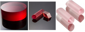
Ti Sapphire Crystal
| Characteristic | Value |
| Chemical formula | Ti3+ Al2O3 |
| Crystal structure | Hexagonal |
| Orientation | A-Axis within 5°,E-vector parallel to C-Axis |
| Mass density | 3.98 g/cm3 |
| Moh’s hardness | 9 |
| Young’s modulus | 335 GPa |
| Tensile strength | 400 Mpa |
| Melting point | 2040 °C |
| Thermal Conductivity | 33 W / (m K) |
| Thermal expansion coefficient | ≈ 5 × 10⁻⁶K-1 |
| Thermal shock resistance coefficient | 790 W/m |
| Refractive index at a wavelength of 633 nm | 1.76 |
| Temperature coefficient of refraction | 13 × 10-6K-1 |
| Mass fraction 0.1% titanium doping concentration | 4.56 × 1019 cm-3 |
| Concentration | (0.05~0.35) wt% |
| End configuration | Flat/Flat or Brewster/Brewster ends Emission |
| Cross section @790 nm | 41 × 10-20 cm2 |
| Coating | The standard coating is R < 5.0% @532 nm per side and R < 0.5% 650 nm to 850 nm per side. Custom coating supported |
| Characteristic | Value |
| Fluorescence | 3.2 µs |
| Emission wavelength tolerance | 660~1100 nm |
| Central radiation | 800 nm |
| Absorption coefficient | 0.5~6.0 cm-1 |
| Central absorption wavelength | 490nm |
| Figure of Merit (FOM) | 100~300 |
| Verticality | 5ˊ |
| Clear aperture | >90% |
| Surface roughness | <λ/8@632 nm |
| Wavefront distortion | <λ/4@632 nm |
Polishing Specification
| Characteristic | Value |
| Orientation Tolerence | < 0.5° |
| Thickness/Diameter Tolerance | ±0.05 mm |
| Surface Flatness | <λ/8@632 nm |
| Wavefront Distortion | <λ/4@632 nm |
| Surface Quality | 10/5 |
| Parallel | 30″ |
| Perpendicular | 15′ |
| Clear Aperture | >90% |
| Chammfer | <0.2×45° |
| Maximum dimensions | dia 150mm |
Standard Product
| Aperture dimension/mm | Length/mm | End surface | Coatings | FOM |
| 6 | 5 | Brewster Cut | – | >120 |
| 10 | >150 | |||
| 15 | >150 | |||
| 20 | >180 | |||
| 5 | Right-angle Cut | (R<1%)@532 nm + (R<0.3%)780-820 nm |
>120 | |
| 10 | >150 | |||
| 15 | >150 | |||
| 20 | >180 | |||
| 6×6 | 5 | Brewster Cut | – | >120 |
| 10 | >150 | |||
| 15 | >150 | |||
| 20 | >180 | |||
| 5 | Right-angle Cut | (R<1%)@532 nm + (R<0.3%)780-820 nm |
>120 | |
| 10 | >150 | |||
| 15 | >150 | |||
| 20 | >180 |

Ti Sapphire Crystal (Absorption & Emission)
For more information, please visit our website: https://www.powerwaywafer.com,
send us email at sales@powerwaywafer.com and powerwaymaterial@gmail.com
Found in 1990, Xiamen Powerway Advanced Material Co., Ltd (PAM-XIAMEN) is a leading manufacturer of semiconductor material in China. PAM-XIAMEN develops advanced crystal growth and epitaxy technologies, manufacturing processes, engineered substrates and semiconductor devices. PAM-XIAMEN’s technologies enable higher performance and lower cost manufacturing of semiconductor wafer.
PAM-XIAMEN develops advanced crystal growth and epitaxy technologies, range from the first generation Germanium wafer, second generation Gallium Arsenide with substrate growth and epitaxy on III-V silicon doped n-type semiconductor materials based on Ga, Al, In, As and P grown by MBE or MOCVD, to the third generation: Silicon carbide and Gallium Nitride for LED and power device application.