PAM XIAMEN offers Thinned Silicon Wafers! We have them! In Stock and ready to ship!
Free Standing Thin Silicon Wafers
We offer freestanding super thin silicon wafers with thicknesses ranging from 5µm to 100µm and with diameters from 5mm to 6. The thin Silicon wafers are true mirror finish DSP, good surface flatness, haze-free, void-free, and have low surface RMS (typical 1-2nm) and an ultralow TTV typically less than +/-1µm.
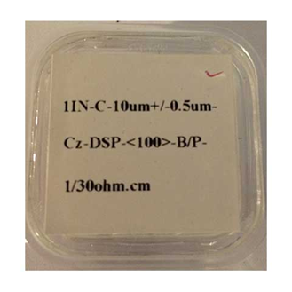
Above Example of Thin Si in Package
Below are just some of out wafers uses.
Lab-On-Chip ELISA
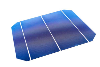
* More efficient Solar Wafers, up to 51%!
* Micro Counter
* Micro-Cantilever Sensing and Actuation Components
* Photo Dynamic Therapy Laser
* Light Engine for Portable Information Display, and
* Dynamic Diagnostics Tools for Light Emitting Devices
PAM XIAMEN along with our partners now specializes optical MEMS and specialty silicon products. These products and services include
· Deformable mirrors for adaptive optics
· Large format ASIC drivers for deformable mirrors
· MEMS, telecom, instrumentations, and piezoelectrics
· Speciality silicon products such as super thin silicon wafers
· Silicon nitride TEM windows/grids
· PMN-PT/Silicon Unimorphs for optics
· MEMS, measurement, and piezoelectric industries
· Wafer services including bonding, coating, grinding/lapping/polishing, and wafer dicing
Wafer Thicknesses of 5um, 10um, 25um, 50um 100um and more!
We have a large in stock inventory of super-thin Silicon ranging from 5um, 25um, 50um and so on.
Our super-thin silicon production is based on a proprietary combination of the following
· Wafer Bonding
· Lapping
· Polishing
· Debodning Process
Diameter/dimension range from <25.4mm – 150mm, larger is some cases.
The thin wafers are haze and void free. They have low surface roughness of 1-2nm and TTV +/-1um.
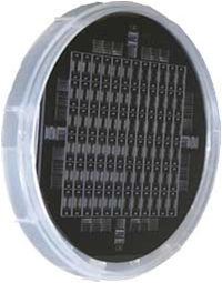
Rigid Wafer Ring for Easy Handling
We can also supply an attachement with rigid wafer ring for our thin silicon wafers. This allows for easy handling.
We can also provide the following services on our thin wafers
· Wafer Dicing
· Silicon wafer lapping and polishing to 5-50um thickness
· Wafer Bonding to mate a cavity wfer with a bare wafer
· PECVD Nitride, LS Nitride, Oxide and LS Oxide on Silicon Including super thin silicon wafers
· Ebeam and thermal evaporation of metal coatings (Ti, Cr, Au, Pt, Pd, Al, Cu, Ag etc) on our wafers including our super-thin wfers
· IC assembly (wafer dicing, die attachment, wire bonding, flip chip bonding)
For more information, please visit our website: https://www.powerwaywafer.com,
send us email at sales@powerwaywafer.com and powerwaymaterial@gmail.com
Found in 1990, Xiamen Powerway Advanced Material Co., Ltd (PAM-XIAMEN) is a leading manufacturer of semiconductor material in China. PAM-XIAMEN develops advanced crystal growth and epitaxy technologies, manufacturing processes, engineered substrates and semiconductor devices. PAM-XIAMEN’s technologies enable higher performance and lower cost manufacturing of semiconductor wafer.
PAM-XIAMEN develops advanced crystal growth and epitaxy technologies, range from the first generation Germanium wafer, second generation Gallium Arsenide with substrate growth and epitaxy on III-V silicon doped n-type semiconductor materials based on Ga, Al, In, As and P grown by MBE or MOCVD, to the third generation: Silicon carbide and Gallium Nitride for LED and power device application.