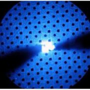
GaN HEMT epitaxy Wafer
Gallium Nitride (GaN) HEMT (Bóng bán dẫn có độ linh động điện tử cao) là thế hệ tiếp theo của công nghệ bóng bán dẫn điện RF. Nhờ công nghệ GaN, PAM-XIAMEN hiện cung cấp tấm wafer AlGaN/GaN HEMT Epi trên sapphire hoặc Silicon và AlGaN/GaN trên mẫu sapphire.
- Sự miêu tả
Mô Tả Sản Phẩm
GaN HEMT epitaxial wafer is a multilayer film grown epitaxially on a substrate, which usually includes a nucleation layer, a transition layer, a buffer layer, a channel layer, a barrier layer, a cap layer, and a passivation layer from bottom to top. The nucleation layer, like AlGaN or AlN, is used to prevent the substrate material from diffusing into the GaN epitaxial layer. The transition layer may contain hierarchical AlGaN, AlN/GaN superlattice or multilayer AlN to balance the stress between the GaN and the substrate. The higher the Al content in the barrier layer of AlGaN, the higher the 2DEG concentration at the heterojunction. Meanwhile, the lower the threshold voltage of the device, and the higher the current capacity. As the Al ratio increasing, the degree of heterogeneous crystal lattice mismatch will be higher, resulting in a decrease in gallium nitride HEMT electron mobility and a decrease in current capacity.
The High Electron Mobility Transistor (HEMT) is developed based on GaN with unique heterostructure and two-dimensional electron gas. The GaN HEMT advantages include high breakdown strength, low on-resistance and faster The switching speed, which is very suitable for medium and low voltage and medium and small power systems, such as travel adapters, wireless chargers, AC-DC converters, smart home appliances, etc. The epitaxial wafer with HEMT structure is more attractive currently for high-frequency converters, in which GaN HEMT breakdown voltage is 600~650 V. With the rapid development of gallium nitride HEMT epi technology, the price of GaN HEMT devices will be competitive, which can gain large GaN HEMT market for GaN HEMT manufacturers. Moreover, due to the gallium nitride HEMT reliability, it can be widely used in industrial fields, such as photovoltaic inverters, energy storage systems, and electric vehicles.
1. GaN HEMT Material: Available size:2”,4”,6”,8”:
More specific parameters of gallium nitride HEMT wafer for D-mode GaN HEMTs, E-mode GaN HEMTs, GaN HEMT power amplifier and RF, please refer to:
We are expert in HEMT structure, we also offer GaN HEMT epi wafer for many years.
For silicon substrate, we need to know if you grow GaN HEMT on silicon for POWER or RF, it is different. If needed, please contact victorchan@powerwaywafer.com for details.
For SiC, you should use semi-insulating.
Or you can buy AlGaN/GaN HEMT structure on these three structure from us.
2. Now we show you an example as follows:
2.1 2 "(50.8mm) GaN HEMT epitaxy Quế
We offer 2″(50.8mm) gallium nitride HEMT Wafers, the GaN HEMT structure is as follows:
Cấu trúc (từ trên xuống dưới):
* GaN nắp undoped (2 ~ 3nm)
AlxGa1-xN (18 ~ 40nm)
AlN (lớp đệm)
un-pha tạp GaN (2 ~ 3um)
Sapphire bề mặt
* Chúng ta có thể sử dụng để thay thế Si3N GaN trên đỉnh, độ bám dính rất mạnh, nó được phủ bởi bắn mực lên hoặc PECVD.
2.2 AlGaN/GaN HEMT Epi Wafer on sapphire/GaN
| lớp # | Thành phần | Độ dày | X | dopant | Carrier Nồng độ |
| 5 | GaN | 2nm | – | – | – |
| 4 | AlxGa1–xN | 8nm | 0.26 | – | – |
| 3 | AlN | 1nm | Un-pha tạp | ||
| 2 | GaN | ≥1000 nm | Un-pha tạp | ||
| 1 | Đệm / chuyển lớp | – | – | ||
| bề mặt | Silicon | 350μm / 625μm | – | ||
2.3 2″(50.8mm),4″ (100mm)AlGaN/GaN HEMT Epi Wafer on Si
2.3.1 Specifications for Aluminium Gallium Nitride (AlGaN) / Gallium Nitride (GaN) Cao Electron Mobility Transistor (HEMT) trên bề mặt Silicon.
| Các yêu cầu | Đặc điểm kỹ thuật |
| AlGaN / GaN HEMT Epi Wafer trên Si | |
| cấu trúc AlGaN / GaN HEMT | Tham khảo 1.2 |
| bề mặt vật liệu | Silicon |
| Sự định hướng | <111> |
| phương pháp tăng trưởng | float Zone |
| Loại dẫn | P hoặc N |
| Kích thước (inch) | 2” , 4” |
| Độ dày (mm) | 625 |
| mặt sau | Thô |
| Điện trở (Ω-cm) | >6000 |
| Bow (mm) | ≤ ± 35 |
2.3.2 Epi structure: Crack-free Epilayers
| lớp # | Thành phần | Độ dày | X | dopant | Carrier Nồng độ |
| 5 | GaN | 2nm | – | – | – |
| 4 | AlxGa1–xN | 8nm | 0.26 | – | – |
| 3 | AlN | 1nm | Un-pha tạp | ||
| 2 | GaN | ≥1000 nm | Un-pha tạp | ||
| 1 | Đệm / chuyển lớp | – | – | ||
| bề mặt | Silicon | 350μm / 625μm | – | ||
2.3.3 Electrical Properties of the AlGaN/GaN HEMT structure
2DEG Mobility (300 K): ≥1,800 cm2 / Vs
2DEG Tấm Carrier Mật độ (ở 300 K): ≥0.9 × 1013 cm-2
RMS Độ nhám bề mặt (AFM): ≤ 0,5 nm (5.0 mm × 5.0 mm quét Area)
2.4 2″(50.8mm)AlGaN/GaN on sapphire
Đối với đặc điểm kỹ thuật của AlGaN / GaN trên mẫu sapphire, xin vui lòng liên hệ với bộ phận bán hàng của chúng tôi: sales@powerwaywafer.com.
GaN HEMT Applications: Used in blue laser diodes, ultraviolet LEDs (down to 250 nm), and AlGaN/GaN HEMTs device.
3. Explanation of AlGaN/Al/GaN HEMTs:
HEMTs nitride đang mạnh mẽ phát triển cho thiết bị điện tử công suất cao trong khuếch đại và chuyển mạch điện ứng dụng tần số cao. Thông thường hiệu suất cao trong hoạt động DC bị mất khi HEMT được bật - ví dụ, sụp đổ trên dòng khi tín hiệu cổng được xung. Người ta cho rằng hiệu ứng như vậy có liên quan đến trách bẫy mà mặt nạ tác động của các cửa khẩu trên dòng chảy hiện tại. Dòng biển đề về nguồn và cổng điện cực đã được sử dụng để thao tác các điện trường trong thiết bị, giảm thiểu hiện tượng vãng sụp đổ như vậy.
4. GaN EpitaxialTechnology — Customized GaN epitaxy on SiC,Si and Sapphire substrate for HEMTs, LEDs:
GAN HEMT epitaxy tấm (GAN EPI-tấm)
PAM XIAMEN Offers Epitaxial growth of AlGaN/GaN based HEMT on Si wafers
5. GaN Device:
GaN HEMT
6. Test Characterization Equipment:
Không tiếp xúc tấm Kháng
Laser Thin Chiều dầy Mapping
Cao Nhiệt độ / Độ ẩm cao Xếp Bias
Sốc nhiệt
DIC Nomarski Kính hiển vi
Atomic Force Microscope (AFM)
Surface Defectivity Scan
Nhiệt độ cao Xếp Bias
4PP Bảng Kháng
Không tiếp xúc sảnh Mobility
Chu kỳ nhiệt độ
Nhiễu xạ tia X (XRD) / số phản xạ (XRR)
Ellipsometer dày
Profilometer
CV Tester
7. Foundry Fabrication:
we also offer foundry GaN HEMT fabrication in the following process as follows:
MOCVD epitaxy
Kim loại phún xạ / E-Beam
Khô / Ướt kim loại / điện môi Etch
Thin Film PECVD / LPCVD / phún xạ
RTA / lò luyện kim
Photolithography (0.35um phút. CD)
Cấy ion
Nhận xét:
Chính phủ Trung Quốc đã công bố các giới hạn mới đối với việc xuất khẩu vật liệu Gallium (như GaAs, GaN, Ga2O3, GaP, InGaAs và GaSb) và vật liệu Germanium dùng để sản xuất chip bán dẫn. Bắt đầu từ ngày 1 tháng 8 năm 2023, chúng tôi chỉ được phép xuất khẩu những nguyên liệu này nếu có giấy phép của Bộ Thương mại Trung Quốc. Rất mong sự thông cảm và hợp tác của bạn!
More fabrication services, please visit: GaN Fabrication Services for HEMT Devices
Aluminium gallium arsenide epi wafer
650V GaN FETs Chip for Fast Charge
GaN MOSFET Structure:
GaN MOSFET Structure on SiC Substrate
More about GaN HEMT structures, please read:
Bạn cũng có thể thích…
-
Ge (Gecmani) Crystal Độc thân và Quế
PAM-XIAMEN cung cấp wafer germanium 2”, 3”, 4” và 6”, viết tắt của wafer Ge do VGF / LEC phát triển. Tấm wafer Germanium loại P và N pha tạp nhẹ cũng có thể được sử dụng cho thí nghiệm hiệu ứng Hall. Ở nhiệt độ phòng, germani kết tinh giòn và ít dẻo. Germanium có tính chất bán dẫn. Germanium có độ tinh khiết cao được pha tạp các nguyên tố hóa trị ba (như indium, gali, boron) để thu được chất bán dẫn germanium loại P; và các nguyên tố hóa trị năm (như antimon, asen và phốt pho) được pha tạp để thu được chất bán dẫn germani loại N. Germanium có đặc tính bán dẫn tốt, chẳng hạn như độ linh động của điện tử cao và độ linh động của lỗ trống cao. -
Float-Zone Mono-tinh thể Silicon
PAM-XIAMEN có thể cung cấp tấm wafer silicon vùng nổi, thu được bằng phương pháp Vùng nổi. Các thanh silicon đơn tinh thể có được thông qua sự phát triển của vùng phao, sau đó xử lý các thanh silicon đơn tinh thể thành các tấm silicon, được gọi là các tấm silicon vùng nổi. Do tấm silicon tan chảy theo vùng không tiếp xúc với nồi nấu kim loại thạch anh trong quá trình silicon vùng nổi nên vật liệu silicon ở trạng thái lơ lửng. Qua đó ít bị ô nhiễm hơn trong quá trình nung chảy silicon vùng nổi. Hàm lượng carbon và hàm lượng oxy thấp hơn, tạp chất ít hơn và điện trở suất cao hơn. Nó phù hợp để sản xuất các thiết bị điện và một số thiết bị điện tử điện áp cao.
-
GaAs Epiwafer
PAM-XIAMEN đang sản xuất nhiều loại vật liệu bán dẫn loại n pha tạp silicon epi wafer III-V dựa trên Ga, Al, In, As và P do MBE hoặc MOCVD phát triển. Chúng tôi cung cấp cấu trúc epiwafer GaAs tùy chỉnh để đáp ứng thông số kỹ thuật của khách hàng, vui lòng liên hệ với chúng tôi để biết thêm thông tin.
-
GaN Templates
Mẫu Sản phẩm PAM-Hạ Môn của bao gồm lớp tinh thể (gallium nitride) GaN mẫu, (nhôm nitrua) mẫu AlN, (gallium nitride nhôm) mẫu AlGaN và (indium gallium nitride) mẫu InGaN, được lắng đọng trên sapphire -
GaSb wafer
PAM-XIAMEN cung cấp tấm bán dẫn hỗn hợp GaSb wafer – gallium antimonide được phát triển bởi LEC (Czochralski đóng gói dạng lỏng) ở dạng sẵn sàng epi hoặc cơ học với loại n, loại p hoặc bán cách điện theo các hướng khác nhau(111) hoặc (100).
-
chất nền GaN freestanding
PAM-Hạ Môn đã thành lập các công nghệ sản xuất cho freestanding (gallium nitride) GaN chất nền wafer, mà là cho UHB-LED và LD. Phát triển bằng công nghệ hydride pha hơi epitaxy (HVPE), bề mặt GaN chúng tôi có mật độ khuyết tật thấp.
-
Chất nền wafer SiC
Công ty có một dây chuyền sản xuất chất nền wafer SiC (silicon cacbua) hoàn chỉnh tích hợp quá trình phát triển tinh thể, xử lý tinh thể, xử lý wafer, đánh bóng, làm sạch và thử nghiệm. Ngày nay, chúng tôi cung cấp các tấm wafer SiC 4H và 6H thương mại có khả năng bán cách nhiệt và dẫn điện trên trục hoặc ngoài trục, kích thước có sẵn: 5x5mm2,10x10mm2, 2”,3”,4”, 6” và 8”, đột phá các công nghệ chủ chốt như như ngăn chặn khuyết tật, xử lý tinh thể hạt giống và tăng trưởng nhanh chóng, thúc đẩy nghiên cứu và phát triển cơ bản liên quan đến epitaxy cacbua silic, thiết bị, v.v.
-
GaN dựa LED epitaxy Wafer
GaN PAM-Hạ Môn của (gallium nitride) dựa trên LED wafer epitaxy là dành cho độ sáng cao điốt phát quang siêu màu xanh và màu xanh lá cây (LED) và điốt laser (LD) ứng dụng.


