
InP wafer
PAM-XIAMEN cung cấp tấm wafer VGF InP(Indium Phosphide) với cấp chính hoặc cấp thử nghiệm bao gồm loại dope thấp, loại N hoặc bán cách điện. Độ linh động của wafer InP khác nhau ở các loại khác nhau, loại có độ pha tạp thấp>=3000cm2/Vs, loại N>1000 hoặc 2000cm2V.s (phụ thuộc vào nồng độ pha tạp khác nhau), loại P: 60+/-10 hoặc 80+/-10cm2 /Vs (phụ thuộc vào nồng độ pha tạp Zn khác nhau) và bán xúc phạm> 2000cm2/Vs, EPD của Indium Phosphide thường dưới 500/cm2.
- Sự miêu tả
Mô Tả Sản Phẩm
InP wafer
PAM-XIAMEN, a leading InP wafer supplier, offers Compound Semiconductor InP wafer – Indium Phosphide which are grown by LEC(Liquid Encapsulated Czochralski) or VGF(Vertical Gradient Freeze) as epi-ready or mechanical grade with n type, p type or semi-insulating. The InP wafer orientation (111) or (100) is available. And the dopants can be Sulphur, Sn(Tin), Zinc or customs. The Laser Mark as specified on backside of InP wafer along with primary flat. The orientation with slight deflection angle is available, such as (100)0.075° towards [110]]±0.025°.
Indium phosphide (InP) is a binary semiconductor composed of indium and phosphorus. It has a face-centered cubic (“zinc blende”) crystal structure, identical to that of GaAs and most of the III-V semiconductors. Indium phosphide can be prepared from the reaction of white phosphorus and indium iodide [clarification needed] at 400 °C., also by direct combination of the purified elements at high temperature and pressure, or by thermal decomposition of a mixture of a trialkyl indium compound and phosphide. Indium phosphide wafers are used in high-power and high-frequency electronics [citation needed] because of the superior electron velocity with respect to the more common semiconductors silicon and gallium arsenide. The InP wafer size we can offer is 2”, 3” and 4”, and the InP wafer thickness will be 350~625um.
Dưới đây là thông số kỹ thuật chi tiết:
| Mục | Specifications | |||
| dopant | N-type | N-type | P-type | SI-type |
| Conduction Type | low doped | Sulphur | Zinc | lron |
| Wafer Diameter | 2″ | |||
| Wafer Orientation | (100)±0.5° | |||
| Wafer Thickness | Min:325 Max:375 | |||
| Primary Flat Length | 16±2mm | |||
| Secondary Flat Length | 8±1mm | |||
| Carrier Concentration | 3×1016cm-3 | (0.8-6)x1018cm-3 | (0.6-6)x1018cm-3 | N/A |
| Mobility | (3.5-4)x103cm2/V.s | (1.5-3.5)x103cm2/V.s | 50-70×103cm2/V.s | >1000cm2/V.s |
| Resistivity | N/A | N/A | N/A | N/A |
| EPD | <1000cm-2 | <500cm-2 | <1×103cm-2 | <5×103cm-2 |
| TTV | <10um | |||
| BOW | <10um | |||
| WARP | <12um | |||
| Laser marking | upon request | |||
| Suface finish | P/E, P/P | |||
| Epi ready | yes | |||
| Package | Single wafer container or cassette | |||
2″ P Type InP Wafer Specification
| Mục | Parameter | UOM |
| Chất liệu | InP | |
| Conduct Type/Dopant | S-C-P/Zn | |
| Cấp | Prime | |
| Diameter: | 50.5±0.4 | mm |
| Orientation: | (100)±0.5° | |
| Orientation Angle: | / | |
| Thickness: | Min:325 Max:375 | um |
| Carrier Concentration: | Min:0.6E18 Max:3E18 | cm-3 |
| Resistivity: | Min:/ Max:/ | ohm.cm |
| Mobility: | Min:/ Max:/ | cm-2/V.sec |
| EPD: | Ave<:1000 Max<:/ | cm-2 |
| TTV: | Max:10 | um |
| TIR: | Max:10 | um |
| BOW: | Max:10 | um |
| Warp: | Max:15 | um |
| Flat Option: | EJ | |
| Primary Flat Orientation: | (0-1-1) | |
| Primary Flat Length: | 16±1 | mm |
| Secondary Flat Orientation: | (0-11) | |
| Secondary Flat Length: | 7±1 | mm |
| Suface: | Side 1:Polished Side 2:etched | |
| Edge Rounding | 0.25(Conform to SEMI Standards) | mmR |
| Particle Count: | / | |
| Package | individual container filled with N2 | |
| Epi-ready | Yes | |
| Laser Marking | Back side major flat | |
| Remark: | Special specifications will be discussed separately | |
3″ InP Wafer Specification
| Mục | Specifications | |||
| dopant | N-type | N-type | P-type | SI-type |
| Conduction Type | low doped | Sulphur | Zinc | lron |
| Wafer Diameter | 3 " | |||
| Wafer Orientation | (100)±0.5° | |||
| Wafer Thickness | 600±25um | |||
| Primary Flat Length | 16±2mm | |||
| Secondary Flat Length | 8±1mm | |||
| Carrier Concentration | ≤3×1016cm-3 | (0.8-6)x1018cm-3 | (0.6-6)x1018cm-3 | N/A |
| Mobility | (3.5-4)x103cm2/V.s | (1.5-3.5)x103cm2/V.s | 50-70×103cm2/V.s | >1000cm2/V.s |
| Resistivity | N/A | N/A | N/A | N/A |
| EPD | <1000cm-2 | <500cm-2 | <1×103cm-2 | <5×103cm-2 |
| TTV | <12um | |||
| BOW | <12um | |||
| WARP | <15um | |||
| Laser marking | upon request | |||
| Suface finish | P/E, P/P | |||
| Epi ready | yes | |||
| Package | Single wafer container or cassette | |||
4″ InP Wafer Specification
| Mục | Specifications | |||
| dopant | N-type | N-type | P-type | SI-type |
| Conduction Type | low doped | Sulphur | Zinc | lron |
| Wafer Diameter | 4″ | |||
| Wafer Orientation | (100)±0.5° | |||
| Wafer Thickness | 600±25um | |||
| Primary Flat Length | 16±2mm | |||
| Secondary Flat Length | 8±1mm | |||
| Carrier Concentration | ≤3×1016cm-3 | (0.8-6)x1018cm-3 | (0.6-6)x1018cm-3 | N/A |
| Mobility | (3.5-4)x103cm2/V.s | (1.5-3.5)x103cm2/V.s | 50-70×103cm2/V.s | >1000cm2/V.s |
| Resistivity | N/A | N/A | N/A | N/A |
| EPD | <1000cm-2 | <500cm-2 | <1×103cm-2 | <5×103cm-2 |
| TTV | <15um | |||
| BOW | <15um | |||
| WARP | <15um | |||
| Laser marking | upon request | |||
| Suface finish | P/E, P/P | |||
| Epi ready | yes | |||
| Package | Single wafer container or cassette | |||
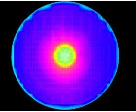
PL(Photoluminescence) Test of indium Phosphide Wafer
We measure InP wafers by Peak Lambda, Peak int, and FWHM, the spectra mapping is as follows:

About InP Wafer Application
As a new type of compound semiconductor material, InP wafer market share is increasing gradually. Due to the excellent indium phosphide properties, the performance of microwave power source devices, microwave amplifiers and gate FETs fabricated on InP material will be better than those fabricated on existing gallium arsenide materials. Indium phosphide heterojunction lasers are also extremely promising light sources in optical fiber communications.
InP wafer fabrication for devices, like growing millimeter wave microelectronic devices and optoelectronic device materials for optical fiber communications, is widely used. With the continuous improvement of device performance and the reduction of device size, the quality requirements for indium phosphide wafers are getting higher and higher. Therefore, the InP wafer process is optimizing gradually.
The the typical values is see below data:
| Peak Lambda(nm) | Peak Int | FWHM(nm) |
| 1279.4 | 7.799 | 48.5 |
| 1279.8 | 5.236 | 44.6 |
Bạn cũng có thể thích…
-
InSb wafer
PAM-XIAMEN cung cấp tấm wafer InSb bán dẫn hỗn hợp - tấm wafer antimonide indium được phát triển bởi LEC (Czochralski đóng gói dạng lỏng) dưới dạng cấp epi hoặc cơ học với loại n, loại p hoặc bán cách điện theo các hướng khác nhau (111) hoặc (100). Indium antimonide pha tạp isoelectronic (chẳng hạn như pha tạp N) có thể làm giảm mật độ khuyết tật trong quá trình sản xuất màng mỏng indium antimonide.
-
chất nền GaN freestanding
PAM-Hạ Môn đã thành lập các công nghệ sản xuất cho freestanding (gallium nitride) GaN chất nền wafer, mà là cho UHB-LED và LD. Phát triển bằng công nghệ hydride pha hơi epitaxy (HVPE), bề mặt GaN chúng tôi có mật độ khuyết tật thấp.
-
SiC epitaxy
Chúng tôi cung cấp phim tùy chỉnh mỏng (silicon carbide) SiC epitaxy trên 6H hoặc 4H chất nền cho sự phát triển của các thiết bị silicon carbide. SiC epi wafer được sử dụng chủ yếu cho điốt Schottky, oxit kim loại bán dẫn transistor hiệu ứng trường, hiệu ứng trường ngã ba -
GaP wafer – Không thể cung cấp tạm thời
PAM-XIAMEN cung cấp tấm wafer GaP bán dẫn hỗn hợp - tấm wafer gallium phosphide được phát triển bởi LEC (Czochralski đóng gói dạng lỏng) ở dạng sẵn sàng epi hoặc cơ học với loại n, loại p hoặc bán cách điện theo các hướng khác nhau (111) hoặc (100). -
GaSb wafer
PAM-XIAMEN cung cấp tấm bán dẫn hỗn hợp GaSb wafer – gallium antimonide được phát triển bởi LEC (Czochralski đóng gói dạng lỏng) ở dạng sẵn sàng epi hoặc cơ học với loại n, loại p hoặc bán cách điện theo các hướng khác nhau(111) hoặc (100).
-
Ge (Gecmani) Crystal Độc thân và Quế
PAM-XIAMEN cung cấp wafer germanium 2”, 3”, 4” và 6”, viết tắt của wafer Ge do VGF / LEC phát triển. Tấm wafer Germanium loại P và N pha tạp nhẹ cũng có thể được sử dụng cho thí nghiệm hiệu ứng Hall. Ở nhiệt độ phòng, germani kết tinh giòn và ít dẻo. Germanium có tính chất bán dẫn. Germanium có độ tinh khiết cao được pha tạp các nguyên tố hóa trị ba (như indium, gali, boron) để thu được chất bán dẫn germanium loại P; và các nguyên tố hóa trị năm (như antimon, asen và phốt pho) được pha tạp để thu được chất bán dẫn germani loại N. Germanium có đặc tính bán dẫn tốt, chẳng hạn như độ linh động của điện tử cao và độ linh động của lỗ trống cao. -
GaAs (Gallium Arsenide) Quế
Là nhà cung cấp chất nền GaAs hàng đầu, PAM-XIAMEN sản xuất Chất nền wafer GaAs (Gallium Arsenide) sẵn sàng Epi bao gồm loại n bán dẫn, loại pha tạp C bán dẫn và loại p với loại chính và loại giả. Điện trở suất của chất nền GaAs phụ thuộc vào chất pha tạp, pha tạp Si hoặc pha tạp Zn là (0,001~0,009) ohm.cm, pha tạp C là >=1E7 ohm.cm. Hướng tinh thể wafer GaAs phải là (100) và (111). Đối với hướng (100), nó có thể lệch 2°/6°/15°. EPD của wafer GaAs thông thường là <5000/cm2 đối với đèn LED hoặc <500/cm2 đối với LD hoặc vi điện tử.
-
Inas wafer
PAM-XIAMEN cung cấp wafer InAs bán dẫn hợp chất – wafer indium arsenide được phát triển bởi LEC (Czochralski đóng gói dạng lỏng) ở dạng sẵn sàng epi hoặc cơ học với loại n, loại p hoặc bán cách điện theo các hướng khác nhau (111) hoặc (100). Ngoài ra, tinh thể đơn InAs có độ linh động điện tử cao và là vật liệu lý tưởng để chế tạo các thiết bị Hall.