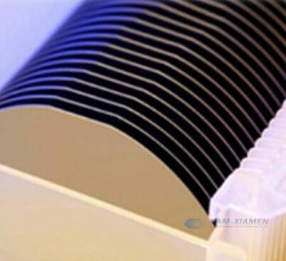
Through continuous efforts, PAM-XIAMEN has developed large-scale COP-free CZ silicon (Si) wafers, and effectively controlled the generation of COP in the ingot by improving the thermal field of crystal pulling, thereby achieving performance improvement and power consumption reduction. The 8-inch silicon wafer application process is larger, so it is not sensitive to COP; the 12-inch silicon wafer application process is smaller and more sensitive to crystal quality. Generally speaking, the process below 40nm has higher requirements on crystal quality, so there is more demand for COP-Free. The specifications of COP free wafer for sale are as follows:
1. COP Free Wafer Data Sheet
| Types of COP Free Wafer | Polished | Annealed | Epitaxy |
| Diameter | 8” & 12” | 12” | 8” & 12” |
| Orientation | (100), (110) or (111) | ||
| Conduction Type | N & P | ||
2. What is COP of CZ-Si Wafer?
COP (crystal originated particles/pits) is primary defect in silicon single crystal. This defect is a lattice defect revealed after boil-polishing silicon wafers with SC-1 (NH4OH:H2O2:H2O-1:1 5) solution at 85 °C for 4 hours. After treating the silicon wafer with SC-1 solution, the surface layer of the silicon wafer was etched away by 150 nm. The density of COP defects can be detected by a laser scanning particle counter.
COP defects are octahedral micro-voids, as shown in Figure 1, the size of COP is 0.12~0.30um. The etch pits of COP defects can generally be divided into two categories: one is monotype, the other is bitype.
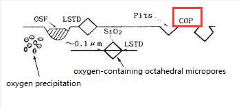
Fig. 1 Schematic of COP Defects
3. Why do CZ Wafers Have COP Defects?
The formation of the primary defect COP is closely related to the formation of oxygen precipitation. The reasons are:
(1) The large primary defects in CZ silicon have not been found in oxygen-free FZ silicon;
(2) On the basis of the calculation of the free energy of microvoids, it is proved that microvoids cannot form uniformly from bare vacancies;
(3) During CZ silicon growth, over a fairly wide temperature range, oxygen is supersaturated and therefore precipitates. Using the energy dispersive X-ray spectrum of TEM, elemental analysis of COP defects can be performed, and it is found that some COP defects contain oxygen. This indicates that the mechanism of void formation is also related to oxygen precipitation.
In addition, the growth rate of COP defects is the fastest in the range of 900~1100 °C, so the time spent in this temperature range determines the size of the growth of COP defects. Rapidly passing through this temperature region can effectively prevent the growth of COP defects. However, since single crystals tend to grow within a certain pulling speed range, such as the pulling speed of heavily doped Sb is generally 0.6-1.2 mm/min. And the general thermal field temperature range of 900 ~ 1100 ° C is wider, so the COP defect size is bound to grow during the entire growth process of the single crystal. The size of COP defects is also affected by the cleaning times of the subsequent wafer processing. After cleaned in SC1 for 5-6 times, the number and size of COP defects increase exponentially.
4. How to Obtain Crystal-Originated-Pits-Free Wafer?
There have been many research literatures in eliminating or decreasing the COPs to get COP-free substrates, which can be summarized as:
(1) Generate nitrogen-doped silicon single crystal;
(2) Hydrogen or argon annealing to eliminate surface COP defects;
(3) Adjust the longitudinal temperature of the thermal field Gradient, reducing COP defect density and shrinking COP defect size.
Some studies have pointed out that when the concentration of dopant boron exceeds a critical value, the generation of COP will be effectively suppressed, then getting COP-free crystal wafers. The size of this critical value is related to the diameter of the ingot. For example, for a 200mm silicon ingot, the critical value is 4.8×10¹⁸ atom/cm3; for a 150mm ingot, it is 6.3×10¹⁸ atom/cm3.
Studies have also shown that high-temperature annealing in hydrogen and argon atmospheres can effectively reduce hole-type micro-defects (such as COPs) on the surface of silicon wafers, thereby improving the GOI for MOS device applications. Since the surface of the silicon wafer (including the surface of the COP) is covered with a layer of natural oxide, whether using a hydrogen atmosphere or an argon atmosphere, under high temperature, as long as the silicon wafer is heated to a high temperature of about 1200°C, the natural oxide layer on the surface of the wafer becomes thermally unstable and dissociates to generate additional silicon atoms. These extra silicon atoms will fill the positions of the COPs, so that these hole-type micro-defects gradually become smaller or even disappear, thereby obtaining silicon COP free wafer or low COP Si wafer.

For more information, please contact us email at victorchan@powerwaywafer.com and powerwaymaterial@gmail.com.