Fabrication of GaN wafers for electronic and optoelectronic devices
The fabrication of GaN wafers from GaN boules (ingots) is described. Gallium nitride boules were grown by hydride vapor phase epitaxy and sliced and sized into wafer blanks. The GaN wafer blanks were lapped and polished. The gallium-side of the wafer was finished with a chemical mechanical polish (CMP) process, which removed surface and subsurface damage, yielding GaN wafers ready for homoepitaxial growth. The CMP polished surface produced a root-mean-square (RMS) surface roughness of 0.3 nm on a 10 × 10 μm2 scan area.
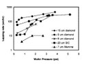
Fig. 1. Lapping rate as a function of pressure on the GaN wafer blank for five different abrasive materials on a cast iron plate. All other operation conditions were kept constant.
Source: Current Applied Physics
If you need more information about Fabrication of GaN wafers for electronic and optoelectronic devices, please visit our website:https://www.powerwaywafer.com/, send us email at sales@powerwaywafer.com or powerwaymaterial@gmail.com