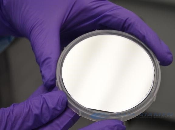
GaAs (gallim arsenide) epitaxial wafer with specific growth for high voltage (HV) diode stacks can be provided by PAM-XIAMEN. Gallium arsenide structure provides required power density, efficiency and reliability for extremely compact systems. GaAs diode wafers meet the requirements for power electronics in modern industrial applications, power generation from renewable energies, or all-electric or hybrid vehicles. Especially in the medium and high voltage range between 600 and 1700 volts, GaAs epitaxial growth increases energy efficiency while also reducing the weight, size and overall cost of the corresponding complete system. Following is the specification of GaAs epitaxy with an unusual and very thick growth:
1. Specification of GaAs Epitaxy
| GaAs Homoepitaxy for HV Diodes PAMP16076-GAAS | ||||
| Layer | Material | Doping Concentration | Thickness | Mark |
| Substrate | GaAs n-doped | 2×1018 cm-3 | – | thickness not relevant > 250microns |
| Epi 1 | GaAs n-doped | – | 5 microns | – |
| Epi 2 | GaAs p-doped | (1-3)E15 | – | – |
| Epi 3 | GaAs p-doped | – | – | – |
Notes for GaAs homoepitaxial films:
Thickness deviation of each layer: +/-10%;
Concentration deviation of each layer: +/-30%;
Total thickness: 15um.
LPE (liquid phase epitaxy) technology solutions can make the growing process of diode structure with high efficiency, and high quality GaAs epilayers can be obtained.
2. P-Type Doping GaAs Epitaxy on GaAs Substrate
GaAs epi wafer with high p-type doping concentration is widely used in devices such as bipolar transistors. Among p-type doped GaAs semiconductor materials, Be is an ideal p-type dopant source with many advantages. Be used as a dopant source can prepare highly doped GaAs epiwafer with controllable doping concentration to meet the requirements of the device. At the same time, Be is also a typical p-type doping source in AlGaAs, InGaAs material system devices. Be used as a p-type doping source for high-concentration doping has good advantages in device applications, such as low-resistance heterojunction bipolar transistors, p-type unalloyed ohmic contacts, etc.
There are a large number of dangling bonds on the surface of GaAs, and GaAs and As oxides are easily formed when exposed to air. These oxides will form non-radiative recombination centers and reduce the luminescence properties of GaAs materials. Therefore, reducing the surface non-radiative recombination center and surface state density of GaAs materials is of great significance to improve the luminescence performance of GaAs-based devices. Sulfur passivation is an effective treatment method to improve the luminescence properties of GaAs. After the GaAs epitaxy is subjected to sulfur passivation treatment, the oxide layer on the surface is removed, and at the same time, Ga and As on the surface combine with S to form sulfide, which reduces the surface state density, improves the radiation recombination on the surface of the epitaxial growth of gallium arsenide, and improves the photoluminescence properties of epitaxy in GaAs.
3. Unstable Growth in GaAs (001) Homoepitaxy
We use atomic force and scanning tunneling microscopy to study MBE grown GaAs (001) epitaxy. When the epitaxial growth conditions favor the island nucleation, the evolution of multilayers can be found. With the thickness of GaAs epistructures increases, the features are grown in all dimensions and the inclination angle keeps at 1°. No bumps occur on surfaces grown in step flow. We surmise the features of multilayers of GaAs epitaxy depend on island nucleation and the existence of step edge barrier because of the unstable growth mode.

For more information, please contact us email at victorchan@powerwaywafer.com and powerwaymaterial@gmail.com.