GaAs (Gallium Arsenide) Quế
Là nhà cung cấp chất nền GaAs hàng đầu, PAM-XIAMEN sản xuất Chất nền wafer GaAs (Gallium Arsenide) sẵn sàng Epi bao gồm loại n bán dẫn, loại pha tạp C bán dẫn và loại p với loại chính và loại giả. Điện trở suất của chất nền GaAs phụ thuộc vào chất pha tạp, pha tạp Si hoặc pha tạp Zn là (0,001~0,009) ohm.cm, pha tạp C là >=1E7 ohm.cm. Hướng tinh thể wafer GaAs phải là (100) và (111). Đối với hướng (100), nó có thể lệch 2°/6°/15°. EPD của wafer GaAs thông thường là <5000/cm2 đối với đèn LED hoặc <500/cm2 đối với LD hoặc vi điện tử.
- Sự miêu tả
Mô Tả Sản Phẩm
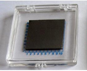
(gallium Arsenide) Bánh xốp GaAs
PAM-XIAMEN phát triển và sản xuất chất nền bán dẫn hỗn hợp-tinh thể gali arsenua và wafer. Chúng tôi đã sử dụng công nghệ tăng trưởng tinh thể tiên tiến, quy trình đóng băng gradient dọc (VGF) và quy trình sản xuất tấm bán dẫn GaAs, thiết lập dây chuyền sản xuất từ tăng trưởng tinh thể, cắt, mài đến xử lý đánh bóng và xây dựng phòng sạch 100 lớp để làm sạch và đóng gói tấm bán dẫn GaAs. Các tấm GaAs của chúng tôi bao gồm các tấm/tấm phôi 2~6 inch cho các ứng dụng LED, LD và Vi điện tử. Chúng tôi luôn tận tâm cải thiện chất lượng của chất nền wafer GaAs hiện tại và phát triển chất nền kích thước lớn. Kích thước wafer GaAs được cung cấp là 2”, 3”, 4” và 6”, và độ dày phải là 220-700um. Hơn nữa, giá wafer GaAs từ chúng tôi là cạnh tranh.
1. Thông số kỹ thuật tấm GaAs
1.1 (GaAs)gallium ArsenideTấm cho các ứng dụng đèn LED
| Mục | Đặc tính kỹ thuật | Các chú thích |
| Loại dẫn | SC / n-type | SC / p-type với Zn dope sẵn |
| Phương pháp phát triển | VGF | |
| dopant | Silicon | Zn có sẵn |
| wafer Diamter | 2, 3 & 4 inch | Phôi hoặc như cắt availalbe |
| Định hướng tinh | (100) 2 °/ 6 ° / 15 ° tắt (110) | misorientation khác có sẵn |
| HÀNH | EJ hoặc Mỹ | |
| Carrier Nồng độ | (0.4 ~ 2.5) E18 / cm3 | |
| Điện trở tại RT | (1,5 ~ 9) E-3 Ohm.cm | |
| Mobility | 1500 ~ 3000cm2 / V.sec | |
| Etch Pit Mật độ | <5000 / cm2 | |
| Laser Marking | theo yêu cầu | |
| Kết thúc bề mặt | P / E hay P / P | |
| Độ dày | 220 ~ 450um | |
| epitaxy Ready | Vâng | |
| gói | Độc wafer container hoặc băng cassette | |
1.2 (GaAs)gallium ArsenideTấm cho các ứng dụng LD
| Mục | Đặc tính kỹ thuật | Các chú thích |
| Loại dẫn | SC / n-type | |
| Phương pháp phát triển | VGF | |
| dopant | Silicon | |
| wafer Diamter | 2, 3 & 4 inch | Phôi hoặc như cắt sẵn |
| Định hướng tinh | (100) 2 °/ 6 ° / 15 ° tắt (110) | misorientation khác có sẵn |
| HÀNH | EJ hoặc Mỹ | |
| Carrier Nồng độ | (0.4 ~ 2.5) E18 / cm3 | |
| Điện trở tại RT | (1,5 ~ 9) E-3 Ohm.cm | |
| Mobility | 1500 ~ 3000 cm2 / V.sec | |
| Etch Pit Mật độ | <500 / cm2 | |
| Laser Marking | theo yêu cầu | |
| Kết thúc bề mặt | P / E hay P / P | |
| Độ dày | 220 ~ 350um | |
| epitaxy Ready | Vâng | |
| gói | Độc wafer container hoặc băng cassette | |
1.3 (GaAs)gallium ArsenideTấm, Semi-cách điện cho Microelectronics Ứng dụng
| Mục | Đặc tính kỹ thuật | Các chú thích |
| Loại dẫn | xốp cách nhiệt | |
| Phương pháp phát triển | VGF | |
| dopant | C doped | |
| wafer Diamter | 2, 3 & 4 inch | phôi có sẵn |
| Định hướng tinh | (100)+/- 0,5° | |
| HÀNH | EJ, Mỹ hoặc notch | |
| Carrier Nồng độ | n / a | |
| Điện trở tại RT | > 1e7 Ohm.cm | |
| Mobility | > 5000 cm2 / V.sec | |
| Etch Pit Mật độ | <8000 / cm2 | |
| Laser Marking | theo yêu cầu | |
| Kết thúc bề mặt | P / P | |
| Độ dày | 350 ~ 675um | |
| epitaxy Ready | Vâng | |
| gói | Độc wafer container hoặc băng cassette | |
1,4 6″ (150mm)(GaAs)gallium ArsenideTấm, Semi-cách điện cho Microelectronics Ứng dụng
| Mục | Đặc tính kỹ thuật | Các chú thích |
| Loại dẫn | Semi-cách điện | - |
| Grow Phương pháp | VGF | - |
| dopant | C doped | - |
| Loại | N | - |
| Diamater (mm) | 150 ± 0,25 | - |
| Sự định hướng | (100)0°±3,0° | - |
| notch Định hướng | 〔010〕±2° | - |
| Notch Deepth (mm) | (1-1,25)mm 89°-95° | - |
| Carrier Nồng độ | vui lòng tham khảo ý kiến đội ngũ bán hàng của chúng tôi | - |
| Điện trở suất (ohm.cm) | >1.0×10⁷ | - |
| Mobility (cm2 / vs) | vui lòng tham khảo ý kiến đội ngũ bán hàng của chúng tôi | - |
| làm rối loạn | vui lòng tham khảo ý kiến đội ngũ bán hàng của chúng tôi | - |
| Độ dày (mm) | 675 ± 25 | - |
| Cạnh trừ cho Bow và Warp (mm) | vui lòng tham khảo ý kiến đội ngũ bán hàng của chúng tôi | - |
| Bow (mm) | vui lòng tham khảo ý kiến đội ngũ bán hàng của chúng tôi | - |
| Warp (mm) | ≤20.0 | - |
| TTV (mm) | ≤10.0 | - |
| TIR (mm) | ≤10.0 | - |
| LFPD (mm) | vui lòng tham khảo ý kiến đội ngũ bán hàng của chúng tôi | - |
| đánh bóng | P / P Epi-Ready | - |
1,5 2″(50,8mm) LT-GaAs (Thấp Nhiệt độ-Grown Arsenua Gali) Wafer Thông số kỹ thuật
| Mục | Đặc tính kỹ thuật |
| Loại dẫn | Semi-cách điện |
| Grow Phương pháp | VGF |
| dopant | Sub:C doped / Epi:Undoped |
| Loại | N |
| Diamater (mm) | 150 ± 0,25 |
| Sự định hướng | (100)0°±3,0° |
| notch Định hướng | 〔010〕±2° |
| Notch Deepth (mm) | (1-1,25)mm 89°-95° |
| Carrier Nồng độ | vui lòng tham khảo ý kiến đội ngũ bán hàng của chúng tôi |
| Điện trở suất (ohm.cm) | >1.0×10⁷ hoặc 0.8-9 x10⁻³ |
| Mobility (cm2 / vs) | vui lòng tham khảo ý kiến đội ngũ bán hàng của chúng tôi |
| làm rối loạn | vui lòng tham khảo ý kiến đội ngũ bán hàng của chúng tôi |
| Độ dày (mm) | 675 ± 25 |
| Cạnh trừ cho Bow và Warp (mm) | vui lòng tham khảo ý kiến đội ngũ bán hàng của chúng tôi |
| Bow (mm) | vui lòng tham khảo ý kiến đội ngũ bán hàng của chúng tôi |
| Warp (mm) | ≤20.0 |
| TTV (mm) | ≤10.0 |
| TIR (mm) | ≤10.0 |
| LFPD (mm) | vui lòng tham khảo ý kiến đội ngũ bán hàng của chúng tôi |
| đánh bóng | P / P Epi-Ready |
2. Ứng dụng & Thị trường wafer GaAs
Gallium arsenide là một vật liệu bán dẫn quan trọng. Nó thuộc về chất bán dẫn hợp chất nhóm III-V và cấu trúc mạng tinh thể hỗn hợp kẽm, với hằng số mạng là 5,65×10⁻¹⁰m, nhiệt độ nóng chảy là 1237°C và khoảng cách vùng cấm là 1,4 electron vôn. Gallium arsenide có thể được chế tạo thành vật liệu bán cách điện có độ bền cao, có thể được sử dụng để chế tạo chất nền mạch tích hợp, máy dò hồng ngoại, máy dò photon gamma, v.v. Do độ linh động điện tử của nó lớn hơn silicon từ 5 đến 6 lần nên chất nền SI GaAs có được sử dụng quan trọng trong việc chế tạo các thiết bị vi sóng và các mạch kỹ thuật số tốc độ cao. Các thiết bị bán dẫn được chế tạo trên gali arsenua có ưu điểm là tần số cao, nhiệt độ cao, hiệu suất ở nhiệt độ thấp, tiếng ồn thấp và khả năng chống bức xạ mạnh, giúp mở rộng thị trường chất nền GaAs.
3. Giấy chứng nhận kiểm tra wafer GaAs có thể bao gồm phân tích bên dưới nếu cần:
1/ Độ nhám bề mặt của Gallium Arsenide kể cả mặt trước và mặt sau (nanomet).
2/Nồng độ pha tạp của Gallium Arsenide(cm-3)
3/EPD của Gali Arsenua (cm-2)
4/Tính di động của Gallium Arsendie(V.sec)
5/ Phân tích nhiễu xạ tia X (đường cong lắc lư) của Gallium Arsenide: Nửa chiều rộng đường cong phản xạ nhiễu xạ
6/ Hiện tượng quang phát quang ở nhiệt độ thấp (phổ phát xạ trong khoảng 0,7-1,0 μm) của Gali Arsenua: Tỷ lệ phát quang exciton trong phổ phát xạ của dải hồng ngoại gần ở nhiệt độ 4K hoặc 5 K và mật độ kích thích quang học là 1 W / cm2
7/Tốc độ truyền hoặc Hệ số hấp thụ: ngay lập tức, chúng ta có thể đo hệ số hấp thụ của GaAs đơn tinh thể ở bước sóng 1064nm: <0,6423 cm-1 và điều này tương ứng với mức truyền tối thiểu là 33,2% cho mẫu trắng dày chính xác 6,5 mm ở bước sóng 1064nm.
Nhận xét:
Chính phủ Trung Quốc đã công bố các giới hạn mới đối với việc xuất khẩu vật liệu Gallium (như GaAs, GaN, Ga2O3, GaP, InGaAs và GaSb) và vật liệu Germanium dùng để sản xuất chip bán dẫn. Bắt đầu từ ngày 1 tháng 8 năm 2023, chúng tôi chỉ được phép xuất khẩu những nguyên liệu này nếu có giấy phép của Bộ Thương mại Trung Quốc. Rất mong sự thông cảm và hợp tác của bạn!
Bạn cũng có thể thích…
-
chất nền GaN freestanding
PAM-Hạ Môn đã thành lập các công nghệ sản xuất cho freestanding (gallium nitride) GaN chất nền wafer, mà là cho UHB-LED và LD. Phát triển bằng công nghệ hydride pha hơi epitaxy (HVPE), bề mặt GaN chúng tôi có mật độ khuyết tật thấp.
-
InP wafer
PAM-XIAMEN cung cấp tấm wafer VGF InP(Indium Phosphide) với cấp chính hoặc cấp thử nghiệm bao gồm loại dope thấp, loại N hoặc bán cách điện. Độ linh động của wafer InP khác nhau ở các loại khác nhau, loại có độ pha tạp thấp>=3000cm2/Vs, loại N>1000 hoặc 2000cm2V.s (phụ thuộc vào nồng độ pha tạp khác nhau), loại P: 60+/-10 hoặc 80+/-10cm2 /Vs (phụ thuộc vào nồng độ pha tạp Zn khác nhau) và bán xúc phạm> 2000cm2/Vs, EPD của Indium Phosphide thường dưới 500/cm2.
-
CdZnTe (CZT) Wafer
Cadmium Kẽm Telluride (CdZnTe hoặc CZT) là một chất bán dẫn mới, cho phép chuyển đổi bức xạ để electron có hiệu quả, nó được sử dụng chủ yếu trong hồng ngoại màng mỏng epitaxy bề mặt, máy dò tia X và thiết bị dò tia gamma CdZnTe. -
Chất nền wafer SiC
Công ty có một dây chuyền sản xuất chất nền wafer SiC (silicon cacbua) hoàn chỉnh tích hợp quá trình phát triển tinh thể, xử lý tinh thể, xử lý wafer, đánh bóng, làm sạch và thử nghiệm. Ngày nay, chúng tôi cung cấp các tấm wafer SiC 4H và 6H thương mại có khả năng bán cách nhiệt và dẫn điện trên trục hoặc ngoài trục, kích thước có sẵn: 5x5mm2,10x10mm2, 2”,3”,4”, 6” và 8”, đột phá các công nghệ chủ chốt như như ngăn chặn khuyết tật, xử lý tinh thể hạt giống và tăng trưởng nhanh chóng, thúc đẩy nghiên cứu và phát triển cơ bản liên quan đến epitaxy cacbua silic, thiết bị, v.v.
-
GaAs Epiwafer
PAM-XIAMEN đang sản xuất nhiều loại vật liệu bán dẫn loại n pha tạp silicon epi wafer III-V dựa trên Ga, Al, In, As và P do MBE hoặc MOCVD phát triển. Chúng tôi cung cấp các cấu trúc tấm đệm GaAs tùy chỉnh để đáp ứng các thông số kỹ thuật của khách hàng, vui lòng liên hệ với chúng tôi để biết thêm thông tin.
-
Float-Zone Mono-tinh thể Silicon
PAM-XIAMEN có thể cung cấp wafer silicon vùng nổi, thu được bằng phương pháp Float Zone. Các thanh silicon đơn tinh thể được tạo ra thông qua quá trình tăng trưởng vùng nổi, sau đó xử lý các thanh silicon đơn tinh thể thành các tấm wafer silicon, được gọi là các tấm wafer silicon vùng float. Vì tấm wafer silicon nóng chảy theo vùng không tiếp xúc với chén thạch anh trong quá trình silicon vùng nổi, nên vật liệu silicon ở trạng thái lơ lửng. Qua đó ít gây ô nhiễm môi trường trong quá trình nung chảy vùng nổi silic. Hàm lượng carbon và hàm lượng oxy thấp hơn, tạp chất ít hơn và điện trở suất cao hơn. Nó phù hợp để sản xuất các thiết bị điện và một số thiết bị điện tử cao áp.
-
Chất cản quang chế tạo nano
PAM-Hạ Môn Cung cấp tấm cản quang với cản quang
-
Ge (Gecmani) Crystal Độc thân và Quế
PAM-XIAMEN cung cấp wafer germanium 2”, 3”, 4” và 6”, viết tắt của wafer Ge do VGF / LEC phát triển. Cũng có thể sử dụng wafer Germanium loại P và N pha tạp nhẹ cho thí nghiệm hiệu ứng Hall. Ở nhiệt độ phòng, gecmani kết tinh giòn và ít dẻo. Germanium có tính chất bán dẫn. Gecmani có độ tinh khiết cao được pha tạp với các nguyên tố hóa trị ba (chẳng hạn như indi, gali, bo) để thu được chất bán dẫn gecmani loại P; và các nguyên tố hóa trị năm (chẳng hạn như antimon, asen và phốt pho) được pha tạp để thu được chất bán dẫn germani loại N. Germanium có các đặc tính bán dẫn tốt, chẳng hạn như độ linh động của điện tử cao và độ linh động của lỗ trống cao.