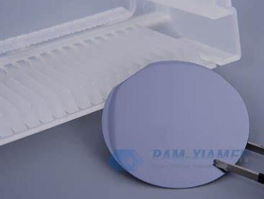
Tấm wafer indium phosphide đơn tinh thể giả có sẵn với pha tạp S do VGF phát triển. Nồng độ điện tử của tấm wafer indium phosphide loại N đạt 1018cm-3, và điện trở suất indium phosphide rất thấp, thường là 10-2~10-3Ω·cm. It is mostly used in high-speed optoelectronic devices, such as LD, LED, PIN- PD, PIN-APD and etc. EPD map of InP can be offered if necessary, please contact us at victorchan@powerwaywafer.com. The specifications of the test grade InP wafers được liệt kê như sau:
1. Thông số kỹ thuật của Indium Phosphide Wafer ở Dummy Grade
Mục 1:
| Mục | Tham số | UOM |
| Chất liệu | Indium Phosphide Wafer | |
| Cấp | Lớp giả | |
| Đường kính | 50,0 ± 0,5 | mm |
| Độ dày | Tối thiểu: 300 Tối đa: 400 | um |
| Sự định hướng | (100) ± 0,5 ° | |
| Loại dẫn điện / Dopant | SCN / S | |
| Tiểu Chiều dài phẳng | 16 ± 2 | mm |
| Định hướng Flat chính | EJ (0-1-1) | |
| Chiều dài phẳng THCS | 7 ± 1 | mm |
| Định hướng Flat Secondary | EJ (0-11) | |
| Carrier Nồng độ | Nhỏ nhất lớn nhất: / | cm-3 |
| Điện trở | Nhỏ nhất lớn nhất: / | ohm-cm |
| Mobility | Nhỏ nhất lớn nhất: / | cm2/ V * Sec |
| EPD | Ave: / Tối đa: <1000 cm-2 | cm-2 |
| TTV | 10 | um |
| TIR | 10 | um |
| CÂY CUNG | 10 | um |
| Làm cong | 15 | um |
| Bề mặt | P / P, P / E | |
| Làm tròn cạnh | 0,25 (Tuân theo Tiêu chuẩn SEMI) | mmR |
| Đã sẵn sàng cho epi | Vâng | |
| Laser Đánh dấu | / | |
| Khu sinh đôi Lamellar | vùng đơn tinh thể hữu ích với (100) định hướng> 80% | |
| gói | thùng chứa cá nhân chứa đầy N2 |
Khoản 2:
| Mục | Tham số | UOM |
| Chất liệu | Chất nền Indium Phosphide | |
| Cấp | Lớp giả | |
| Đường kính | 76,2 ± 0,5 | mm |
| Độ dày | Tối thiểu: 600 Tối đa: 650 | um |
| Sự định hướng | (100) ± 0,5 ° | |
| Loại dẫn điện / Dopant | SCN / S | |
| Tiểu Chiều dài phẳng | 22 ± 1 | mm |
| Định hướng Flat chính | EJ | |
| Chiều dài phẳng THCS | 12 ± 1 | mm |
| Định hướng Flat Secondary | EJ | |
| Carrier Nồng độ | Nhỏ nhất lớn nhất: / | cm-3 |
| Điện trở | Nhỏ nhất lớn nhất: / | ohm-cm |
| Mobility | Nhỏ nhất lớn nhất: / | cm2/ V * Sec |
| EPD | Ave: / Tối đa: <1000 cm-2 | cm-2 |
| TTV | 10 | um |
| TIR | 10 | um |
| CÂY CUNG | 10 | um |
| Làm cong | 15 | um |
| Bề mặt | P / P, P / E | |
| Làm tròn cạnh | 0,25 (Tuân theo Tiêu chuẩn SEMI) | mmR |
| Đã sẵn sàng cho epi | Vâng | |
| Laser Đánh dấu | / | |
| Khu sinh đôi Lamellar | vùng đơn tinh thể hữu ích với (100) định hướng> 80% | |
| gói | thùng chứa cá nhân chứa đầy N2 |
Khoản 3:
| Mục | Tham số | UOM |
| Chất liệu | Indium Phosphide Wafer | |
| Cấp | Lớp giả | |
| Đường kính | 100,0 ± 0,5 | mm |
| Độ dày | Tối thiểu: 600 Tối đa: 650 | um |
| Sự định hướng | (100) ± 0,5 ° | |
| Loại dẫn điện / Dopant | SCN / S | |
| Tiểu Chiều dài phẳng | 32,5 ± 1 | mm |
| Định hướng Flat chính | EJ | |
| Chiều dài phẳng THCS | 18 ± 1 | mm |
| Định hướng Flat Secondary | EJ | |
| Carrier Nồng độ | Nhỏ nhất lớn nhất: / | cm-3 |
| Điện trở | Nhỏ nhất lớn nhất: / | ohm-cm |
| Mobility | Nhỏ nhất lớn nhất: / | cm2/ V * Sec |
| EPD | Ave: / Tối đa: <1000 cm-2 | cm-2 |
| TTV | 10 | um |
| TIR | 10 | um |
| CÂY CUNG | 10 | um |
| Làm cong | 15 | um |
| Bề mặt | P / P, P / E | |
| Làm tròn cạnh | 0,25 (Tuân theo Tiêu chuẩn SEMI) | mmR |
| Đã sẵn sàng cho epi | Vâng | |
| Laser Đánh dấu | / | |
| Khu sinh đôi Lamellar | vùng đơn tinh thể hữu ích với (100) định hướng> 80% | |
| gói | thùng chứa cá nhân chứa đầy N2 |
2. Các ứng dụng Indium Phosphide cấp giả
Tấm wafer InP giả cấp được sử dụng để kiểm tra quá trình tăng trưởng epi và xác định đặc điểm thành phần trên lớp biểu mô. Nó không thích hợp cho các cấu trúc thiết bị khắc, ví dụ như ống dẫn sóng và lưới quang học vì các tinh thể đôi và các lỗ có thể có của định hướng tấm wafer ở mặt đôi.
Microtwin hoặc dòng bề mặt wafer <20% được chấp nhận.
3. Tính chất của Indium Phosphide
Indium phosphide is a group III-V compound semiconductor material compounded by the combination of group III element indium (In) and group V element phosphorus (P). It has a zinc blende structure with a indium phosphide lattice constant of 0.586 9 nm. InP single crystal is soft and brittle, silver-gray with metallic luster. The indium phosphide band gap at room temperature is 1.344 eV, which is a direct transition band structure. The emission wavelength is 0.92 um, the intrinsic carrier concentration of InP at room temperature is 2×107cm-3, và độ linh động của electron và lỗ trống là 4 500 cm2/ Vs và 150 cm2 / V · s tương ứng.

Cấu trúc tinh thể Indium Phosphide
4. Quy trình sản xuất Wafer InP
Indi photphua có cấu trúc tinh thể lập phương tâm mặt gần giống như gali arsenide GaAs và hầu hết các chất bán dẫn III-V. Các tấm xốp Indium phosphide phải được chuẩn bị trước khi sản xuất thiết bị và phải được chồng lên nhau để loại bỏ hư hỏng bề mặt trong quá trình cắt lát. Tấm wafer giả của InP sau đó được đánh bóng cơ học hóa học (CMP) cho công đoạn loại bỏ vật liệu cuối cùng, cho phép tạo ra bề mặt được nhân đôi với độ nhám siêu phẳng quy mô nguyên tử.
However, the growth process of indium phosphide from raw materials to ingots to wafers is very difficult. During the growth process, a high temperature of 1070℃ and extreme pressure are required. In addition, the atomic structure may change. What comes out may not meet expectations. From raw materials to ingots to a 2-inch or 4-inch indium phosphide single crystal wafer, the yield is generally about 28%, and the technical threshold is very high. Therefore, PAM-XIAMEN is one of the indium phosphide wafer suppliers that can successfully control the growth technology of indium phosphide. Relying on VGF, VB method crystal growth technology, high surface quality wire cutting technology, ultra-flat mechanical chemical polishing technology, ultra-clean surface cleaning technology and other related core technologies, the commercialization of indium phosphide wafers tends to be stable, and the products provided by PAM-XIAMEN are mainly used in optical fiber communications, optical detectors, infrared optics, high-frequency millimeter wave communications and other fields. In addition to the current application areas, the monocrystalline indium phosphide wafer substrate will expand in the terahertz field used in 6G communications.
5. Phát triển trong tương lai Vật liệu InP
In fact, InP substrate material is the most critical core material in the optical communication industry chain, ultra-high frequency millimeter wave radar, infrared detection and other fields. It is inseparable from indium phosphide since the demand for higher bandwidth continues to grow, especially in the Human-driven cars, 5G communications, even the implementation and application of 6G, 7G, and 8G in the future. The indium phosphide wafer market at dummy or prime grade will usher in rapid growth, thereby, the indium phosphide wafer cost will go down.

Để biết thêm thông tin, vui lòng liên hệ với chúng tôi qua email victorchan@powerwaywafer.com và powerwaymaterial@gmail.com.