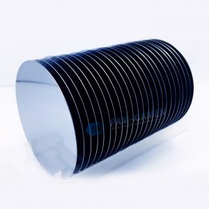
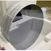
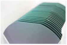
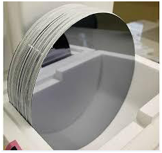
Epitaxy Silicon wafer
Silicon Epiticular Wafer (Epi Wafer) là một lớp tinh thể silicon epiticular được lắng đọng trên một tấm wafer silicon tinh thể đơn (lưu ý: có thể phát triển một lớp lớp Silicon đa tinh thể trên một tấm wafer silicon đơn tinh thể có độ pha tạp cao, nhưng nó cần lớp đệm (như oxit hoặc poly-Si) ở giữa chất nền Si số lượng lớn và lớp silicon epiticular trên cùng. Nó cũng có thể được sử dụng cho bóng bán dẫn màng mỏng.
- Sự miêu tả
Mô Tả Sản Phẩm
Epitaxy Silicon wafer
Silicon epitaxy Wafer(Epi Wafer)là một lớp tinh thể đơn silicon epiticular lắng đọng trên một tinh thểwafer silicon(lưu ý: có thể phát triển một lớp lớp Silicon đa tinh thể trên một tấm wafer silicon đơn tinh thể có độ pha tạp cao, nhưng nó cần lớp đệm (chẳng hạn như oxit hoặc poly-Si) ở giữa chất nền Si số lượng lớn và lớp epiticular trên cùng lớp silicon.Nó cũng có thể được sử dụng cho bóng bán dẫn màng mỏng.
Các phương pháp chuẩn bị tấm silicon epiticular bao gồm epit Wax pha hơi, epit Wax pha lỏng, epit Wax chùm phân tử, v.v. Trong số đó, epit Wax pha hơi dựa trên lắng đọng hơi hóa học (CVD) là quá trình tăng trưởng epiticular silicon chính. Các nguồn thường được sử dụng là SiCl4, SiHCl3, SiH2Cl2 và SiH4.
Để đáp ứng nhu cầu của các thiết bị bán dẫn khác nhau, nhiều công nghệ epiticular silicon khác nhau đã được tạo ra để sản xuất tấm wafer silicon epiticular. Ngoài sự phát triển epiticular silicon trong epit Wax ở nhiệt độ thấp và epit Wax giảm áp suất, còn có epitaxy chọn lọc lắng đọng một lớp epiticular silicon trên một phần cụ thể của tấm wafer silicon.
Các lớp epitaxy có thể được pha tạp, vì nó được gửi, để nồng độ doping chính xác trong khi tiếp tục cấu trúc tinh thể của chất nền.
Epilayer trở suất: <1 ohm-cm lên đến 150 ohm-cm
Epilayer độ dày: <1 um lên đến 150 um
Cấu trúc: N / N +, N / N / N +, N / P / N +, N / N + / P-, N / P / P +, P / P +, P- / P / P +.
Ứng dụng wafer: Digital, Linear, Power, MOS, BiCMOS Thiết bị.
lợi thế của chúng tôi trong nháy mắt
1. Thiết bị tăng trưởng epiticular tiên tiến, thiết bị kiểm tra và công nghệ silicon epiticular.
2.Offer chất lượng cao nhất với mật độ khuyết tật thấp và độ nhám bề mặt tốt.
3.Strong hỗ trợ nhóm nghiên cứu và hỗ trợ kỹ thuật cho khách hàng của chúng tôi
6 "(150mm) Wafer đặc điểm kỹ thuật:
| Mục | Đặc điểm kỹ thuật | |
| bề mặt | Sub đặc tả số | |
| Phương pháp phát triển phôi | CZ | |
| loại dẫn | N | |
| dopant | Như | |
| Sự định hướng | (100) ± 0,5 ° | |
| Điện trở | ≤0.005Ohm.cm | |
| RRG | ≤15% | |
| [Oi] Nội dung | 8 ~ 18 ppma | |
| Đường kính | 150 ± 0,2 mm | |
| Tiểu Chiều dài phẳng | 55 ~ 60 mm | |
| Tiểu Flat Location | {110} ± 1 ° | |
| Chiều dài Thứ hai Flat | bán | |
| Thứ hai Flat Location | bán | |
| Độ dày | 625 ± 15 um | |
| Backside Đặc điểm: | ||
| 1, BSD / Poly-Si (A) | 1.BSD | |
| 2, SiO2 | 2.LTO: 5000 ± 500 A | |
| 3, Edge Exclusion | 3.EE:?0.6 mm | |
| Laser Marking | KHÔNG AI | |
| bề mặt phía trước | Đánh bóng mặt kính | |
| Epi | Kết cấu | N / N + |
| dopant | Phos | |
| Độ dày | 3 ± 0,2 um | |
| Thk.Uniformity | ≤5% | |
| Chức vụ đo lường | Trung tâm (1 pt) 10mm từ mép (4 điểm @ 90 độ) | |
| Phép tính | [Tmax-Tmin] ÷ [[Tmax + Tmin] X 100% | |
| Điện trở | 2,5 ± 0,2 Ohm.cm | |
| Res.Uniformity | ≤5% | |
| Chức vụ đo lường | Trung tâm (1 pt) 10mm từ mép (4 điểm @ 90 độ) | |
| Phép tính | [Rmax-Rmin] ÷ [[Rmax + Rmin] X 100% | |
| Ngăn xếp Mật độ lỗi | ≤2 (ea / cm2) | |
| Sương mù | KHÔNG AI | |
| vết trầy xước | KHÔNG AI | |
| Hố, Orange Peel, | KHÔNG AI | |
| cạnh Thái | ≤1 / 3 Epi dày | |
| Trượt (mm) | Tổng chiều dài ≤ 1Dia | |
| Vấn đề nước ngoài | KHÔNG AI | |
| Trở lại nhiễm bẩn bề mặt | KHÔNG AI | |
| Tổng số khiếm khuyết Point (hạt) | ≤30@0.3um |
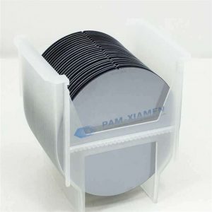
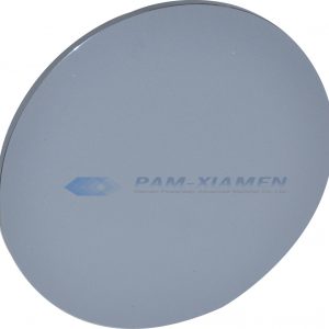
Tấm wafer silicon EPI 4 inch-6
Tấm wafer silicon epiticular 4 inch
Tăng trưởng epit Wax silicon với Boron Dopant của VPE
Tấm wafer silicon cho ống dẫn sóng quang học tích hợp
Bạn cũng có thể thích…
-
Cz Mono-tinh thể Silicon
PAM-XIAMEN, một nhà sản xuất silicon số lượng lớn đơn tinh thể, có thể cung cấp các tấm silicon đơn tinh thể <100>, <110> và <111> với chất dẫn xuất N&P có kích thước 76,2~200 mm, được trồng bằng phương pháp CZ. Phương pháp Czochralski là phương pháp tăng trưởng tinh thể, được gọi là phương pháp CZ. Nó được tích hợp trong một hệ thống nhiệt ống thẳng, được làm nóng bằng điện trở than chì, làm tan chảy polysilicon chứa trong nồi nấu kim loại thạch anh có độ tinh khiết cao, sau đó đưa tinh thể hạt vào bề mặt nóng chảy để hàn. Sau đó, tinh thể hạt quay được hạ xuống và tan chảy. Thân được xâm nhập và chạm vào, nâng lên dần dần và hoàn thiện hoặc kéo qua các bước thắt cổ, thắt cổ, nắn vai, kiểm soát đường kính bằng nhau và hoàn thiện.
-
khắc wafer
Các tấm silicon khắc do PAM-XIAMEN cung cấp là tấm khắc loại N hoặc loại P, có độ nhám thấp, độ phản xạ thấp và độ phản xạ cao. Tấm wafer khắc có đặc điểm là độ nhám thấp, độ bóng tốt và chi phí tương đối thấp, thay thế trực tiếp tấm wafer được đánh bóng hoặc tấm wafer epiticular có chi phí tương đối cao để sản xuất các bộ phận điện tử trong một số lĩnh vực, giảm chi phí.
-
wafer đánh bóng
PAM-XIAMEN có thể cung cấp tấm wafer được đánh bóng, loại n hoặc loại p với định hướng <100>, <110> hoặc <111>. Tấm wafer được đánh bóng FZ, chủ yếu để sản xuất bộ chỉnh lưu silicon (SR), bộ chỉnh lưu điều khiển bằng silicon (SCR), Transitor khổng lồ (GTR), thyristor (GRO)
-
Kiểm tra Wafer Monitor Wafer Dummy Wafer
Với tư cách là nhà sản xuất wafer giả, PAM-XIAMEN cung cấp wafer giả silicone / wafer thử nghiệm / wafer giám sát, được sử dụng trong thiết bị sản xuất để cải thiện độ an toàn khi bắt đầu quá trình sản xuất và được sử dụng để kiểm tra giao hàng và đánh giá hình thức quy trình. Vì các tấm silicon giả thường được sử dụng để thí nghiệm và kiểm tra nên kích thước và độ dày của chúng là những yếu tố quan trọng trong hầu hết các trường hợp. Tấm wafer giả 100mm, 150mm, 200mm hoặc 300mm có sẵn.
-
GaAs Epiwafer
PAM-XIAMEN đang sản xuất nhiều loại vật liệu bán dẫn loại n pha tạp silicon epi wafer III-V dựa trên Ga, Al, In, As và P do MBE hoặc MOCVD phát triển. Chúng tôi cung cấp cấu trúc epiwafer GaAs tùy chỉnh để đáp ứng thông số kỹ thuật của khách hàng, vui lòng liên hệ với chúng tôi để biết thêm thông tin.
-
Float-Zone Mono-tinh thể Silicon
PAM-XIAMEN có thể cung cấp tấm wafer silicon vùng nổi, thu được bằng phương pháp Vùng nổi. Các thanh silicon đơn tinh thể có được thông qua sự phát triển của vùng phao, sau đó xử lý các thanh silicon đơn tinh thể thành các tấm silicon, được gọi là các tấm silicon vùng nổi. Do tấm silicon tan chảy theo vùng không tiếp xúc với nồi nấu kim loại thạch anh trong quá trình silicon vùng nổi nên vật liệu silicon ở trạng thái lơ lửng. Qua đó ít bị ô nhiễm hơn trong quá trình nung chảy silicon vùng nổi. Hàm lượng carbon và hàm lượng oxy thấp hơn, tạp chất ít hơn và điện trở suất cao hơn. Nó phù hợp để sản xuất các thiết bị điện và một số thiết bị điện tử điện áp cao.
-
GaN Templates
Mẫu Sản phẩm PAM-Hạ Môn của bao gồm lớp tinh thể (gallium nitride) GaN mẫu, (nhôm nitrua) mẫu AlN, (gallium nitride nhôm) mẫu AlGaN và (indium gallium nitride) mẫu InGaN, được lắng đọng trên sapphire -
SiC epitaxy
Chúng tôi cung cấp phim tùy chỉnh mỏng (silicon carbide) SiC epitaxy trên 6H hoặc 4H chất nền cho sự phát triển của các thiết bị silicon carbide. SiC epi wafer được sử dụng chủ yếu cho điốt Schottky, oxit kim loại bán dẫn transistor hiệu ứng trường, hiệu ứng trường ngã ba


Những sảm phẩm tương tự
-
Tấm wafer silicon cao cấp 12″
PAM-XIAMEN cung cấp tấm silicon trần 300mm (12 inch) ở loại cao cấp, loại n hoặc loại p và độ dày tấm silicon 300mm là 775±15. So với các nhà cung cấp wafer silicon khác, giá wafer silicon của Powerway Wafer cạnh tranh hơn và chất lượng cao hơn. Tấm silicon 300mm có năng suất trên mỗi tấm wafer cao hơn so với tấm silicon có đường kính lớn trước đây.
-
Tấm wafer silicon 12″ cấp thử nghiệm
PAM-XIAMEN cung cấp tấm silicon trần 300mm (12 inch), loại thử nghiệm, loại n hoặc loại p. So với các nhà cung cấp wafer silicon khác, Powerway Wafer cung cấp dịch vụ chuyên nghiệp với giá cả cạnh tranh.
-
Tấm silicon 12 inch 300mm TOX (Tấm xốp oxy hóa nhiệt Si)
PAM-XIAMEN cung cấp tấm wafer silicon oxit và wafer dioxide 300mm. Tấm wafer silicon oxit nhiệt hoặc wafer silicon dioxide là một tấm wafer silicon trần với lớp oxit được hình thành bằng quá trình oxy hóa khô hoặc ướt. Lớp oxit nhiệt của tấm wafer silicon thường được trồng trong lò ống nằm ngang và phạm vi nhiệt độ oxit của tấm wafer silicon thường là 900oC ~ 1200oC. So với lớp oxit CVD, lớp oxit wafer silicon có độ đồng đều cao hơn, độ nén tốt hơn, độ bền điện môi cao hơn và chất lượng tốt hơn.