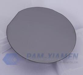
PAM-XIAMEN can provide wafer polishing service for III-V compound wafers (such as InSb wafer, GaSb wafer, InAs wafer), ultra-thin semiconductor wafer, CZT wafer and other photoelectric materials. We aim to adopt a high-precision chemical polishing process to minimal surface damage. Take the InSb wafer polishing process for example:
1. Wafer Polishing Capability for InSb
The wafer polishing method of PAM-XIAMEN is designed to reduce the surface roughness and remove surface damage to obtain a mirror-like InSb wafer substrate. The polished InSb wafers we can obtain are:
| Surface Process | Double Side Polished |
| Surface Roughness | Ra<0.5nm |
| TTV | <5um |
| Warp | <8um |
| Bow | <5um |
| Thickness after Polishing | 500um |
| surface Atomic Ratio | ≈1 |
2. Why InSb Wafer Needs Polishing ?
Infrared detectors based on indium antimonide materials are being developed in units, 1D arrays and 2D focal plane arrays. With the increase of the number of detector pixels, the important quality factors such as the sound rate, noise, response time of the detector not only depend on the semiconductor parameters such as carrier concentration, mobility, lifetime and so on of the InSb wafer, but also the surface state of the InSb chip. Among which, the increase of surface roughness will increase the noise of the device. Moreover, the density of the surface dangling bonds will increase, which will enhance the surface attraction, and it will be easier to adsorb metal ions, which will lead to the decline of the electrical properties of the InSb chip, and the leakage current will be greatly increased. Thereby, the surface roughness will affect the performance of the device. This friction will bring a certain degree of machine damage to the InSb chip. Therefore, to eliminate this mechanical damage, InSb wafer surface polishing is required.
The staring-type focal plane array enables modern infrared photoelectric systems to achieve excellent performance in terms of temperature sensitivity, spatial resolution and temporal resolution, and makes the system more portable and reliable. Therefore, the InSb semiconductor material requires no scratches on the surface and the roughness is less than 3A. Excessive scratches and excessive roughness will affect the sensitivity of the device. So polishing a wafer is necessary.
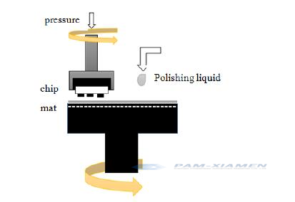
Diagram of CMP Equipment
3. Challenges for Polishing InSb Wafer
Due to the low hardness of InSb wafer compared to other semiconductor materials, the surface state is not easy to control during grinding and polishing, and surface damage such as cracks, pits and orange peels, as well as sub-surface damage such as phase transitions, dislocations and residual stress, are prone to occur. Thus, it will lead to the increase of surface state density and dark current. Therefore, the grinding and polishing process has been a key process for the fabrication of InSb devices, especially mid-wave infrared focal plane detectors. The semiconductor wafer polishing process urgently needs to be improved and researched. The research on the surface state of InSb materials is relatively rare in the entire industry, and there is also a lack of certain standards. Compared with the quality of InSb material, the level of grinding and polishing technology restricts the uniformity and yield improvement of InSb focal plane detectors.

For more information, please contact us email at victorchan@powerwaywafer.com and powerwaymaterial@gmail.com.