PAM-XIAMEN participates in the design and processing of MEMS and compound semiconductor GaAs microwave integrated circuit (GaAs MMIC) devices, and focuses on the research, development, production and service of micro-nano sensors, micro-electromechanical systems (MEMS), micro-nano manufacturing and compound semiconductor GaAs chips. We are a high-tech enterprise offering wafer processing service, specializing in the research, development and manufacturing of MEMS (Micro Electro Mechanical System) sensors, and have the international advanced level of micro-nano design and processing capabilities. We can realize the wafer production, packaging and testing of various MEMS sensors. The products developed by wafer semiconductor process include uncooled infrared detectors, pressure sensors, microfluidics, gas sensors and other MEMS sensors. Compound semiconductor GaAs integrated circuit products include strained heterojunction high mobility transistor (pHEMT) power, low noise and GaAs photoconductive switch and other chip processing services.
Besides, PAM-XIAMEN as one of wafer processing companies undertakes the manufacturing and single-step and multi-step processing services of various semiconductor devices such as MEMS and GaAs, such as silicon wafer thermal oxidation, ion implantation, photolithography, RIE etching, PECVD, LPCVD, magnetron sputtering, electron beam evaporation, deep silicon etching, rapid annealing, electroplating, cutting, bonding, packaging and other wafer foundry services. Supply all kinds of silicon wafers, single/double polished wafers, oxide silicon wafers, coated wafers, ultra-thick wafers, ultra-thick oxide wafers, metal-plated wafers, cut wafers, GaAs & GaP wafers, GaN wafers, sapphire wafers, etc.
Following are services of wafer to chip process offered by us:
1. MEMS Two-Dimensional Material Integration Service
Our wafer processing techniques can realize the transfer of two-dimensional materials on MEMS.
2. Processing Service for MEMS and Semiconductor Tape Out
Process development and tape-out services of semiconductor chips (for example: DMOS; L-IGBT; MOSFET; PHEMT; HFET; SiC diode; SiC radio frequency chip, etc.) can be offered
Process development and tape-out services of MEMS chips (microfluidics/gas sensors/pressure sensors, etc.) are available as well.
3. Polyimide Process
Polyimide (PI) is made of pyromellitic dianhydride (PMDA) and diaminodiphenyl ether (DDE) in a strong polar solvent through polycondensation and casting into a film, and then imidization. Polyimide has excellent high and low temperature resistance, electrical insulation, adhesion, dielectric resistance, mechanical properties and radiation resistance. It can be used for a long time in the temperature range of -269℃-280℃, and can be reached high temperature of 400℃ in a short time. We masters two types of device processing technology, PI dry film and PI glue, to provide customers with high-quality technical services.
3.1 Polyimide Wafer Processing Technology Application
As a special engineering material, polyimide is widely used in aviation, aerospace, microelectronics, nanometer, liquid crystal, separation membrane, laser and other fields.
3.2 PI Processing Service Capability
Dry film: thickness 20-150um, etching depth ≤15um;
Photosensitive solution: minimum line width 5um, thickness 5-20um;
Non-photosensitive solution: etching depth 0-15um.
3.3 Advantages of PI Processing Service
We have dry film & PI glue processing technology, dry film etching depth can reach 15um, and master multilayer PI film stacking process, good adhesion.
4. Wafer Etching Process
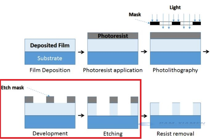
Etch is a technology that selectively etches the surface of the semiconductor substrate or the surface covering film according to the mask pattern or design requirements. It is one very important step of the semiconductor wafer manufacturing process, microelectronic IC manufacturing process and micro-nano manufacturing process. It is one of main wafer processing solutions of pattern processing associated with photolithography. Etching processing servcie is divided into dry etching and wet etching. PAM-XIAMEN currently masters a variety of etching processes, and will design etching solutions with good etching effects and cost-effective according to customer needs.
Etching in Semiconductor Wafer Fabrication Process
4.1 Etching Technology Application
Our etching technology is mainly used in the processing of semiconductor devices, integrated circuit manufacturing, thin film circuits, printed circuits and other fine patterns.
4.2 Etching Processing Capability
Etching technology: ion beam etching, deep silicon etching, reactive ion etching, focused ion beam and other etching technologies;
Etching materials: silicon, silicon oxide, silicon nitride, metal, quartz and other materials
4.3 Advantages of Our Etching Service
* Master a variety of etching techniques;
* Wide range of etching materials;
* The maximum aspect ratio of deep silicon etching is 20:1 with high etching accuracy and small line width.
5. Coating Processing Service
Vacuum coating is refers to the deposition of a certain metal or non-metal on the surface of the material in the form of a gas phase in a vacuum environment to form a dense film. The quality of the coating is critical to the function formation of semiconductor devices.
5.1 Coating Technology Application
Wafer processing metallization is mainly used in the manufacturing process of micro-nano semiconductor devices. Metal and ITO materials are mainly used for the preparation of electrodes, and other non-metallic materials are mainly used for the preparation of insulating dielectric layers and sacrificial mask layers.
5.2 Process Capability of Coating
Master coating technology: Electron beam evaporation magnetron sputtering, LPCVD, PECVD, ALD, MOCVD and MBE.
5.3 Coating Materials
We can do coating with following materials:
Metals: Ti, Al, Ni, Au, Ag, Mo, Cr, Pt, Cu, Ta, TiW, Pd, Zn, W, Nb;
Non-metals: Si, SiO2, SiNx, TiN, Ga2O3, Al2O3, TiO2, HfO2, MgF2, ITO, Ta2O5;
Piezo Film: AlN, PZT, ZnO;
Coating substrates: silicon wafers, quartz glass wafers, sapphire wafers, silicon carbide, II-IIII group substrate, III-V group substrate, PET, Pi, etc.
5.4 Coating Processing Service Advantages
* Master a variety of coating technologies and a wide range of coating materials.
* Coating thickness range: 5nm-10um;
* The base size is 8 inches downward compatible. The coating uniformity is good and the coating is dense.
6. Photolithography Processing
Photolithography is an important step in the manufacturing process of semiconductor devices. The device structure is depicted on the photoresist layer by exposure and development, and then the pattern on the mask is transferred to the substrate through an etching process. We currently possess various lithography wafer processing steps, such as electron beam lithography, step lithography, and contact lithography.
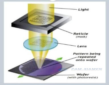
Photolithography Wafer Processing
6.1 Lithography Technology Application
Lithography technology is mainly used in the manufacturing process of semiconductor devices and integrated circuits.
6.2 Wafer Processing Capacity of Photolithography
EBL (Electron Beam Lithography): The minimum CD value is 50nm, and the accuracy can reach 10%.
Stepper: the minimum CD value is 350nm, the exposure error is ±0.1um, and the maximum exposure area is 6 inches.
Contact and proximity lithography: SUSS MA6/BA6 lithography machine, minimum CD value 2um, exposure error ±0.3um
6.3 Photolithography Advantages
* Customize the most cost-effective lithography solution according to customer needs;
* High precision and small line width;
* Substrate size range from 1cm to 8 inches;
* High graphic fidelity.
7. TSV Technology
TSV technology is the abbreviation of through silicon via technology, which is an advanced wafer processing solution for stacking chips in three-dimensional integrated circuits to achieve interconnection. Because TSV processing service can maximize the stacking density of chips in the three-dimensional direction, the shortest interconnection lines between chips, the smallest size, and greatly improve the performance of chip speed and low power consumption, it has become the most eye-catching one in current electronic wafer level packaging technology.
Because of the limitations of process shrinkage and low dielectric value materials, 3D stacking technology is regarded as the key to the ability to manufacture high-performance chips in a smaller size, and through silicon vias (TSV) can integrate wafer stacking through vertical conduction. Achieving the circuit interconnection between chips helps to improve the integration and efficiency of the wafer process systems at a lower cost, and is an important way to realize the 3D integration of integrated circuits. We have a complete TSV process to meet your requirements for chip interconnection.
8. Corrosion Technology
PAM-XIAMEN offers corrosion service, including oxide, nitride, silicon, polysilicon, and germanium isotropic corrosion, standard metal corrosion, non-standard insulating medium, semiconductor and metal corrosion, photoresist removal and silicon wafer cleaning steps, silicide corrosion, plastics and polymer etching, silicon anisotropic etching, bulk silicon and silicon germanium self-stop corrosion, electrochemical corrosion and self-stop, photo-assisted corrosion and self-stop, thin film self-stop corrosion, sacrificial layer removal, porous silicon formation.
9. Wafer Bonding Technology
Bonding is a technology in which two pieces of homogeneous or heterogeneous semiconductor materials with clean and atomic-level flat surfaces undergo surface cleaning and activation treatments, and are directly bonded under certain conditions. The wafers are bonded together through van der Waals force, molecular force or even atomic force. We provide chip to wafer bonding processing service as follows:
– Anodic bonding (pyrex glass and silicon wafer);
– Eutectic bonding (PbSn, AuSn, CuSn, AuSi, etc.), solder is provided by the customer;
– Glue bonding (AZ4620, SU8) , Bonding special glue);
– Wire bonding and others.
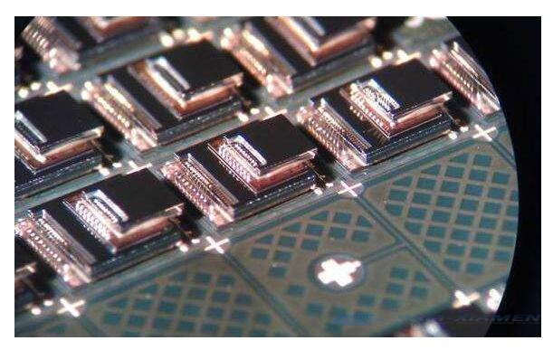
10. Packaging Technology
PAM-XIAMEN provides processing service for fast packaging of MPW engineering chips. The packaging types include COB fast sealing, ceramic package fast sealing and resin package fast sealing, including but not limited to the following package types DIP, SOP, TSSOP, SOT, TO, QFN, DFN , LGA, COB, BGA, QFP, LCC, etc.
Airtight packaging processing service such as AuSn welding and parallel seam welding of ceramic shells can be done. Chip grinding, polishing, mechanical blade cutting, silicon wafer laser non-marking cutting, gold wire bonding, laser welding, chip mounting, dispensing coating, reflow soldering, flip-chip soldering, parallel sealing soldering, BGA ball implanting, tensile shear Shear force test, scanning electron microscope SEM inspection, X-Ray ray inspection, ultrasonic scanning non-destructive inspection and surface roughness inspection, etc.
11. Detection Technology
We have a variety of detection technologies, including TEM, SEM, XRD, AFM, XPS, XRD, ultrasound microscope, X-ray, step meter, profiler, film thickness meter, Raman, etc.

For more information, please contact us email at victorchan@powerwaywafer.com and powerwaymaterial@gmail.com.