Unusual defects, generated by wafer sawing: Diagnosis, mechanisms and how to distinguish from related failures
In the wafer sawing process, unusual failures were observed and their root causes have been investigated. Besides classical and well-known failures, the following failure mechanisms were found. Surface-ESD (ESDFOS), caused by charged water drops and friction electricity of blue carrier foils, ultrasonic cleaning-induced splittering of small surface structures and EEPROM memory loss. Some examples allow valuable conclusions for failure analysis and perform hints how to reduce or eliminate the problem by tool modifications.
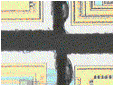
Fig. 1. Chipping-a border- or corner-crack caused by the wafer sawing.
Source: Microelectronics Reliability
If you need more information about Unusual defects, generated by wafer sawing: Diagnosis, mechanisms and how to distinguish from related failures, please visit our website:https://www.powerwaywafer.com/, send us email at sales@powerwaywafer.com or powerwaymaterial@gmail.com.