For non-cubic crystals, they are inherently anisotropic, that is, different directions have different properties. Take the silicon carbide crystal faces for example as below:
- The space groups of 4H-SiC and 6H-SiC are P63mc, and the point group is 6mm. Both belong to the hexagonal system and have anisotropy.
- The space group of 3C-SiC is F-43m and the point group is -43m. It belongs to the cubic crystal system and does not have anisotropy.
- The space group of 15R-SiC is R3m, and the point group is 3m. It belongs to the trigonal crystal system and has anisotropy.
Furthermore, 6mm and 3m belong to one of the 10 polar point groups (1, 2, 3, 4, 6; m, 3m; mm2, 4mm, 6mm), so 4H-SiC, 6H-SiC, 15R-SiC are polar crystals. The polar crystal means that at least one direction in a crystal has different properties from the opposite direction, which can be electrical properties (thermoelectric properties, ferroelectric properties), growth properties, etc. In a word, there will be a difference in performance between the positive and the negative in the same direction.
The expression of anisotropy will be directly reflected in the different properties of different crystal planes. In crystals, different silicon carbide crystal faces are represented by differences in crystal plane indices. The crystal face index is also called the Miller index, which is (hkl).
The specific representation is: establishing the coordinate system of the crystal, the intercept of this crystal face and the coordinate axis will be a, b, c, and then take the reciprocal of the intercept 1/a, 1/b, 1/c, and reduce to the simplest integer ratio, which is (hkl). For crystals of the trigonal and hexagonal crystal system, (hkl) = (hkil), i=-h-k. However, according to the symmetry of the crystal, there will be a series of silicon carbide crystal faces that are the same. For example, (100) and (200) are just not reduced to the simplest integer ratio.
There are many applications for anisotropy.
The growth properties of seed crystals in different directions are very different. Taking the crystal face (0001) as the reference, the wafer deflected by a certain angle (step flow) is easier to grow silicon carbide.
There are also huge differences in the nature of electricity. For example, the silicon carbide crystal face (0-33-8) is used to prepare silicon carbide MOSFET. Due to its lower interface state density and higher free electron ratio, the surface has the highest channel mobility at all doping concentrations.
As shown in the figure, when a doping concentration of 10^18/cm3 is used, a high channel mobility of 60cm2V-1s-1 and a threshold voltage as high as 4V can be achieved—this voltage is sufficient to suppress false start at high temperatures. It is higher than the (0001) crystal plane.
.jpg)
Using this property, a Japanese company developed a new structure for SiC MOSFET. It has a V-shaped groove and uses (0-33-8) crystal planes, thus having higher mobility performance.
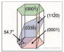
The (0-33-8) crystal plane of 4H-SiC with the (0001) plane forms an off-angle of 54.7 degrees.
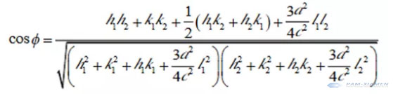
The unit cell parameters of the trigonal and hexagonal crystal systems are a and c. The calculation method of crystal plane (h1k1l1) (h2k2l2) is as follows:
The key to producing this device is to use a chemical etching process to form a V-shaped trench. Use silicon dioxide as an etching mask, and perform etching in a chlorine atmosphere at about 900°C.
- Oxidize the unetched surface to silicon dioxide firstly;
- Chlorine reacts with silicon carbide on the surface to convert it into carbon, and then reacts with oxygen to form carbon dioxide;
- The generated silicon chloride and carbon dioxide volatilize at high temperature, exposing the (0-33-8) crystal plane.
Note: ion etching cannot be used. Although ion etching is a general method for forming U-shaped trenches, it will cause etching damage and the formation of sub-trenches.
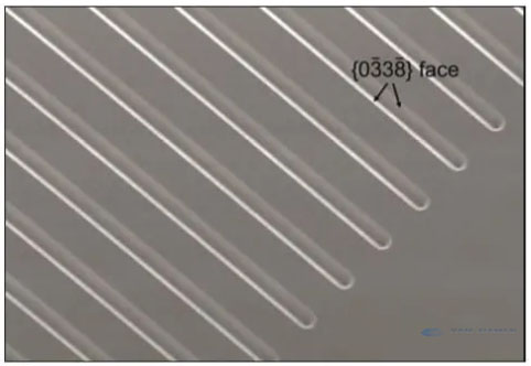
Through the image of scanning electron microscope, it can be seen that the chemical etching has obtained high-quality crystal planes.

For more information, please contact us email at victorchan@powerwaywafer.com and powerwaymaterial@gmail.com.