The development stages of semiconductor wafers are elemental semiconductor, compound semiconductor and wide bandgap semiconductor, as shown in the Fig. 1. Semiconductor wafers can be divided into narrow band gap semiconductors and wide band gap semiconductors according to different band gaps. Wide Band Gap semiconductors (WBG or WBGS) are semiconductor materials with relatively large band gaps compared to typical semiconductors. A typical semiconductor such as silicon has a band gap of 1-1.5 electron volts (eV), while a broadband gap material has a band gap of 2-4 eV. In general, wideband gap semiconductors have electronic properties between typical semiconductors and insulators. SiC and GaN are typical Wide Band Gap materials. PAM-XIAMEN can supply both narrow and wide band gap semiconductor wafers.
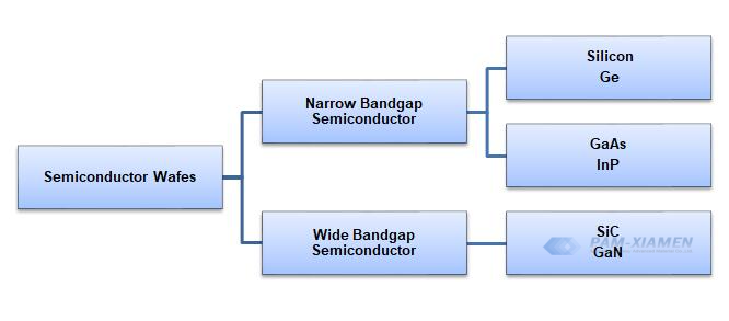
Fig. 1 Semiconductor Wafers Classification based on Bandgap
1. Comparison of Main Performance Parameters of Semiconductor Materials
| First Stage | Second Stage | Third Stage | ||
| Narrow Band Gap | Wide Band Gap | |||
| Si | GaAs | SiC | GaN | |
| Bandgap (eV) | 1.12 | 1.4 | 3.2 | 3.39 |
| Relative Dielectric Constant | 11.7 | 13.1 | 9.7 | 9.8 |
| Dielectric Breakdown Field Strength (MV/cm) | 0.3 | 0.4 | 2.2 | 3.3 |
| Thermal Conductivity (W/cm*K) | 1.5 | 0.5 | 4.5 | 2~3 |
| Electron Mobility (cm2/Vs) | 1350 | 8500 | 900 | 1000 |
| Electron Saturation Drift Velocity (107 cm/s) | 1 | 2 | 2 | 2.5 |
| Power Density (W/mm) | 0.2 | 0.5 | ~10 | >30 |
2. Applications of Wide Bandgap Semiconductor Materials
Compared with silicon, GaN has the characteristics of high critical magnetic field, high electron saturation speed and extremely high electron mobility. It is an excellent choice for ultra-high frequency devices and is suitable for applications in 5G communication, microwave radio frequency and other fields. Take the RF application for example. We offer GaN on Si epitaxial wafer for your reference, link: https://www.powerwaywafer.com/gan-on-si-for-rf.html.
The wide band gap materials have been regarded as a new driving force for the development of today’s electronics industry. The excellent properties similar to GaN make SiC devices suitable for high-frequency and high-temperature application scenarios. Compared with silicon devices, silicon carbide devices can significantly reduce switching losses. Therefore, silicon carbide can manufacture high-voltage, high-power power electronic devices such as MOSFETs, IGBTs, SBDs, etc., which are used in smart grids, new energy vehicles and other industries. PAM-XIAMEN supplies SiC wafer for IGBT devices, more please refer to https://www.powerwaywafer.com/sic-igbt-wafer.html.
Judging from the current research on wide-bandgap semiconductor materials and devices, most of the research focuses on SiC and GaN technologies. SiC technology is the most mature and research progress is also rapid; while GaN technology is widely studied, especially in the application of optoelectronic devices. There are few reports on the wide-bandgap semiconductor technology such as AlN and diamond, but from the perspective of material superiority, it has considerable development potential. It is believed that with the continuous deepening of research, its application prospects will be very broad.

For more information, please contact us email at victorchan@powerwaywafer.com and powerwaymaterial@gmail.com.