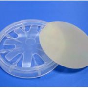

GaN Templates
- وصف
وصف المنتج
الجاليوم Template (gallium nitride template)
PAM-XIAMEN’s GaN Template consists of crystalline layers of gallium nitride (GaN), aluminum nitride (AlN), aluminum gallium nitride (AlGaN) and indium gallium nitride (InGaN), which are epilayer on sapphire and electronic grade for fabrication as MOS-based devices. PAM-XIAMEN’s Gallium Nitride Template Products enable 20-50% shorter epitaxy cycle times and higher quality epitaxial device layers, with better structural quality and higher thermal conductivity,which can improve devices in the cost, yield, and performance.
2″(50.8mm) قوالب الجاليوم Epitaxy on Sapphire Substrates
| بند | PAM-2inch-GaNT-N | PAM-2inch-GaNT-SI |
| نوع التوصيل | N-نوع | شبه العازلة |
| المقوي | Si doped or low doped | الحديد مخدر |
| حجم | 2 "(50MM) ديا. | |
| سماكة | 4um,20um,30um,50um,100um | 30um، 90um |
| اتجاه | C-محور (0001) +/- 1 ° | |
| المقاومة (300K) | <0.05Ω · سم | >1×10⁶Ω·cm |
| خلع الكثافة | <1x108cm-2 | |
| هيكل الركيزة | GaN on Sapphire(0001) | |
| صقل الأسطح | واحد أو ضعف الجانب المصقول، برنامج التحصين الموسع جاهزة | |
| منطقة قابلة للاستخدام | ≥ 90٪ | |
2″ (50.8mm)GaN Templates Epitaxy on Sapphire Substrates
| بند | PAM-غانت-P | |
| نوع التوصيل | P-نوع | |
| المقوي | مخدر ملغ | |
| حجم | 2 "(50MM) ديا. | |
| سماكة | 5um من، 20um، 30um، 50um، 100um | |
| اتجاه | C-محور (0001) +/- 1 ° | |
| المقاومة (300K) | <1Ω · سم أو حسب الطلب | |
| المقوي تركيز | 1E17(cm-3) or custom | |
| هيكل الركيزة | GaN on Sapphire(0001) | |
| صقل الأسطح | واحد أو ضعف الجانب المصقول، برنامج التحصين الموسع جاهزة | |
| منطقة قابلة للاستخدام | ≥ 90٪ | |
3″(76.2mm)GaN Templates Epitaxy on Sapphire Substrates
| بند | PAM-3inch-GaNT-N |
| نوع التوصيل | N-نوع |
| المقوي | Si doped |
| منطقه الاستبعاد: | 5MM من القطر الخارجي |
| Thickness: | 20um,30um |
| Dislocation density | < 1x108cm-2 |
| ورقة المقاومة (300K): | <0.05Ω · سم |
| المادة المتفاعلة: | sapphire |
| Orientation : | C-plane |
| سمك الياقوت: | 430um |
| تلميع: | جانب واحد مصقول، برنامج التحصين الموسع جاهزة، مع الخطوات ذرية. |
| طلاء المؤخر: | (custom)high quality Titanium coating, thickness > 0.4 μm |
| التعبئة والتغليف: | Individually packed under argon |
| Atmosphere vacuum sealed in class 100 clean room. |
3″(76.2mm)GaN Templates Epitaxy on Sapphire Substrates
| بند | PAM-3inch-GaNT-SI |
| نوع التوصيل | شبه العازلة |
| المقوي | Fe Doped |
| منطقه الاستبعاد: | 5MM من القطر الخارجي |
| Thickness: | 20um، 30um، 90um (20um هو الأفضل) |
| Dislocation density | < 1x108cm-2 |
| ورقة المقاومة (300K): | >106 ohm.cm |
| المادة المتفاعلة: | sapphire |
| Orientation : | C-plane |
| سمك الياقوت: | 430um |
| تلميع: | جانب واحد مصقول، برنامج التحصين الموسع جاهزة، مع الخطوات ذرية. |
| طلاء المؤخر: | (custom)high quality Titanium coating, thickness > 0.4 μm |
| التعبئة والتغليف: | Individually packed under argon Atmosphere vacuum sealed in class 100 clean room. |
4″(100mm)GaN Templates Epitaxial on Sapphire Substrates
| بند | PAM-4inch-GaNT-N |
| نوع التوصيل | N-نوع |
| المقوي | low doped |
| Thickness: | 4um |
| Dislocation density | < 1x108cm-2 |
| ورقة المقاومة (300K): | <0.05Ω · سم |
| المادة المتفاعلة: | sapphire |
| Orientation : | C-plane |
| سمك الياقوت: | – |
| تلميع: | جانب واحد مصقول، برنامج التحصين الموسع جاهزة، مع الخطوات ذرية. |
| التعبئة والتغليف: | Individually packed under argon Atmosphere |
| vacuum sealed in class 100 clean room. |
2″ (50.8mm)AlGaN, InGaN, AlN Epitaxy on Sapphire Templates: custom
2”(50.8mm)AlN Epitaxy on Sapphire Templates
| بند | PAM-AlNT-SI |
| نوع التوصيل | semi-insulating |
| قطر | Ф 50.8mm ± 1MM |
| Thickness: | 1000nm +/- 10٪ |
| المادة المتفاعلة: | sapphire |
| Orientation : | C-محور (0001) +/- 1 ° |
| التوجه شقة | طائرة |
| XRD FWHM من (0002) | <200 arcsec. |
| صالحة للاستخدام المساحة بالمتر المربع | ≥90% |
| Polishing: | لا شيء |
2”(50.8mm)InGaN Epitaxy on Sapphire Templates
| بند | PAM-INGAN |
| Conduction Type | – |
| قطر | Ф 50.8mm ± 1mm |
| Thickness: | 100-200nm, custom |
| المادة المتفاعلة: | sapphire |
| Orientation : | C-axis(0001)+/-1O |
| المقوي | في |
| Dislocation Density | ~ 108 cm-2 |
| Useable Surface Area | ≥90% |
| Surface Finish | Single or Double Side Polished,epi-ready |
2”(50.8mm)AlGaN Epitaxy on Sapphire Templates
| بند | PAM-AlNT-SI |
| نوع التوصيل | semi-insulating |
| قطر | Ф 50.8mm ± 1MM |
| Thickness: | 1000nm +/- 10٪ |
| المادة المتفاعلة: | sapphire |
| Orientation : | C-الطائرة |
| التوجه شقة | طائرة |
| XRD FWHM من (0002) | <200 arcsec. |
| صالحة للاستخدام المساحة بالمتر المربع | ≥90% |
| Polishing: | لا شيء |
GaN Template on Sapphire& Silicon
2″(50.8mm)GaN on 4H or 6H SiC substrate
| 1)Undoped GaN buffer or AlN buffer are available; | ||||
| 2)n-type(Si doped or low doped), p-type or semi-insulating GaN epitaxial layers available; | ||||
| 3)vertical conductive structures on n-type SiC; | ||||
| 4)AlGaN – 20-60nm thick, (20%-30%Al), Si doped buffer; | ||||
| 5)GaN n-type layer on 330µm+/-25um thick 2” wafer. | ||||
| 6) Single or double side polished, epi-ready, Ra<0.5um | ||||
| 7)Typical value on XRD: | ||||
| Wafer ID | Substrate ID | XRD(102) | XRD(002) | سماكة |
| #2153 | X-70105033 (with AlN) | 298 | 167 | 679um |
| Single or double side polished, epi-ready, Ra<0.5um | ||||
6″ (150mm)n-GaN on double-side polished flat sapphire
| Target | remark | |
| Substrate diameter | 150 mm | +/- 0.15 mm |
| Substrate thickness | 1300 um or 1000um | +/- 25 um |
| c-plane (0001), offcut angle towards m-plane | 0.2 deg | +/- 0.1 deg |
| Single primary flat length | 47.5 mm | +/- 1 mm |
| Flat orientation | طائرة | +/- 0.2 deg |
| Si-doped n-GaN thickness | 4 um | +/- 5% |
| Si concentration in n-GaN | 5e18 cm-3 | yes |
| u-GaN thickness | 1 um | no this layer |
| XRD rocking curve (002) | < 250 arcsec | <300 arcsec |
| XRD rocking curve (102) | < 250 arcsec | <350 arcsec |
| Dislocation density | < 5e8 cm-2 | yes |
| Front side surface, AFM (5×5 um2) Ra | < 0.5 nm, Epi-ready | yes |
| Back side surfac\e | 0.6 – 1.2 um, fine ground | yes |
| Wafer bowing | < 100 um | no this data |
| n-GaN resistivity (300K) | < 0.01 ohm-cm2 | yes |
| Total thickness variation | < 25 um | <10um |
| Defect density | Macro defects (>100 um):< 1/wafer Micro defects (1-100 um):< 1/cm2 | Macro defects (>100 um):< 10/wafer Micro defects (1-100 um):< 10/cm2 |
| Laser marking | on the backside of the wafer flat | yes |
| Package | packaged in a class 100 clean room environment, in cassettes of 25 pcs or single wafer containers, under nitrogen atmosphere, double sealed | yes |
| Edge exclusion | < 3 mm | yes |
| Useable surface area | > 90% | yes |
Hydride Vapour Phase Epitaxy (HVPE) process
GaN template on sapphire is grown by HVPE process and technology for the production of compound semiconductors such as GaN, AlN, and AlGaN. GaN templates are used in a wide applications: nanowire growth, solid state lighting, short wavelength optoelectronics and RF power device.
In the HVPE process, Group III nitrides (such as GaN, AlN) are formed by reacting hot gaseous metal chlorides (such as GaCl or AlCl) with ammonia gas (NH3). The metal chlorides are generated by passing hot HCl gas over the hot Group III metals. All reactions are done in a temperature controlled quartz furnace.
Remark:
The Chinese government has announced new limits on the exportation of Gallium materials (such as GaAs, GaN, Ga2O3, GaP, InGaAs, and GaSb) and Germanium materials used to make semiconductor chips. Starting from August 1, 2023, exporting these materials is only allowed if we obtains a license from the Chinese Ministry of Commerce. Hope for your understanding and cooperation!
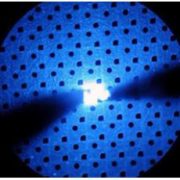
We will offer test reports, please see below an example:
AlGaN template structure report
More products:
GaN Thin Film on Sapphire (Al2O3) Template
ربما يعجبك أيضا…
-
الغاليوم Epiwafer
تقوم شركة PAM-XIAMEN بتصنيع أنواع مختلفة من مواد أشباه الموصلات من النوع n المطلية بالسيليكون epi wafer III-V استنادًا إلى Ga وAl وIn وAs وP المزروعة بواسطة MBE أو MOCVD. نحن نوفر هياكل Epiwafer GaAs المخصصة لتلبية مواصفات العملاء، يرجى الاتصال بنا للحصول على مزيد من المعلومات.
-
شركة جنرال الكتريك (الجرمانيوم) بلورات واحدة ويفر
تقدم شركة PAM-XIAMEN رقائق الجرمانيوم مقاس 2 و3 و4 بوصات و6 بوصات، وهي اختصار لرقائق Ge التي تنمو بواسطة VGF / LEC. يمكن أيضًا استخدام رقاقة الجرمانيوم من النوع P وN المخدرة بشكل خفيف في تجربة تأثير هول. في درجة حرارة الغرفة، يكون الجرمانيوم البلوري هشًا وله القليل من اللدونة. الجرمانيوم له خصائص أشباه الموصلات. يتم تطعيم الجرمانيوم عالي النقاء بعناصر ثلاثية التكافؤ (مثل الإنديوم والجاليوم والبورون) للحصول على أشباه موصلات الجرمانيوم من النوع P؛ ويتم تخدير العناصر الخماسية التكافؤ (مثل الأنتيمون والزرنيخ والفوسفور) للحصول على أشباه موصلات الجرمانيوم من النوع N. يتمتع الجرمانيوم بخصائص جيدة لأشباه الموصلات، مثل حركة الإلكترون العالية وحركة الفتحات العالية. -
اختبار رقاقة مراقب يفر الدمية يفر
باعتبارها شركة مصنعة للرقاقات الوهمية، تقدم PAM-XIAMEN رقاقة السيليكون الوهمية / رقاقة الاختبار / رقاقة المراقبة، والتي يتم استخدامها في جهاز الإنتاج لتحسين السلامة في بداية عملية الإنتاج وتستخدم لفحص التسليم وتقييم نموذج العملية. نظرًا لأن رقائق السيليكون الوهمية غالبًا ما تستخدم للتجربة والاختبار، فإن حجمها وسمكها يعدان من العوامل المهمة في معظم المناسبات. تتوفر الرقاقات الوهمية 100 مم، 150 مم، 200 مم، أو 300 مم.
-
طليق الركيزة الجاليوم
PAM-XIAMEN has established the manufacturing technology for freestanding (gallium nitride)GaN substrate wafer, which is for UHB-LED and LD. Grown by hydride vapour phase epitaxy (HVPE) technology,Our GaN substrate has low defect density.
-
LED الفوقي رقاقة الجاليوم مقرها
PAM-XIAMEN’s GaN(gallium nitride)-based LED epitaxial wafer is for ultra high brightness blue and green light emitting diodes (LED) and laser diodes (LD) application.
-
ركيزة رقاقة SiC
The company has a complete SiC(silicon carbide) wafer substrate production line integrating crystal growth, crystal processing, wafer processing, polishing, cleaning and testing. Nowadays we supply commercial 4H and 6H SiC wafers with semi insulation and conductivity in on-axis or off-axis, available size:5x5mm2,10x10mm2, 2”,3”,4”, 6” and 8″, breaking through key technologies such as defect suppression, seed crystal processing and rapid growth, promoting basic research and development related to silicon carbide epitaxy, devices, etc.
-
الجاليوم HEMT الفوقي ويفر
Gallium Nitride (GaN) HEMTs (High Electron Mobility Transistors) are the next generation of RF power transistor technology. Thanks to GaN technology, PAM-XIAMEN now offer AlGaN/GaN HEMT Epi Wafer on sapphire or Silicon, and AlGaN/GaN on sapphire template.
-
إيناس رقاقة
PAM-XIAMEN offers Compound Semiconductor InAs wafer – indium arsenide wafer which are grown by LEC(Liquid Encapsulated Czochralski) as epi-ready or mechanical grade with n type, p type or semi-insulating in different orientation(111) or (100). In addition, InAs single crystal has high electron mobility and is an ideal material for making Hall devices.