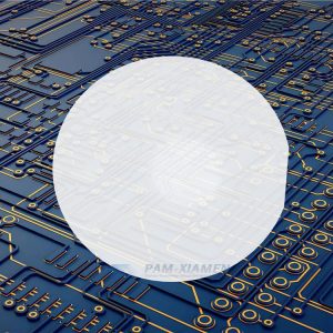

GaN Templates
- Description
Product Description
GaN Template (gallium nitride template)
PAM-XIAMEN’s GaN Template consists of crystalline layers of gallium nitride (GaN), aluminum nitride (AlN), aluminum gallium nitride (AlGaN) and indium gallium nitride (InGaN), which are epilayer on sapphire and electronic grade for fabrication as MOS-based devices. PAM-XIAMEN’s Gallium Nitride Template Products enable 20-50% shorter epitaxy cycle times and higher quality epitaxial device layers, with better structural quality and higher thermal conductivity,which can improve devices in the cost, yield, and performance.
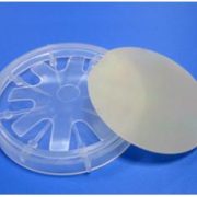
2″(50.8mm) Modèles GaN Epitaxy on Sapphire Substrates
| Article | PAM-2inch-GaNT-N | PAM-2inch-GaNT-SI |
| Type de Conduction | De type N | Semi-isolante |
| dopant | Si doped or low doped | Fe dopés |
| Taille | 2 "(50 mm) de diamètre. | |
| Épaisseur | 4um,20um,30um,50um,100um | 30um, 90um |
| Orientation | C-axe (0001) +/- 1 ° | |
| Résistivité (300K) | <0.05Ω · cm | >1×10⁶Ω·cm |
| Densité de Dislocation | <1x108cm-2 | |
| Structure du substrat | GaN on Sapphire(0001) | |
| Finition de surface | Simple ou double côté poli, epi-prêt | |
| Surface utile | ≥ 90% | |
2″ (50.8mm)GaN Templates Epitaxy on Sapphire Substrates
| Article | PAM-P-GANT | |
| Type de Conduction | De type P, | |
| dopant | mg dopée | |
| Taille | 2 "(50 mm) de diamètre. | |
| Épaisseur | 5um, 20um, 30um, 50um, 100um | |
| Orientation | C-axe (0001) +/- 1 ° | |
| Résistivité (300K) | <1Ω · cm ou sur mesure | |
| Concentration dopant | 1E17(cm-3) or custom | |
| Structure du substrat | GaN on Sapphire(0001) | |
| Finition de surface | Simple ou double côté poli, epi-prêt | |
| Surface utile | ≥ 90% | |
3″(76.2mm)GaN Templates Epitaxy on Sapphire Substrates
| Article | PAM-3inch-GaNT-N |
| Type de Conduction | De type N |
| dopant | Si doped |
| Zone d'exclusion: | 5 mm de diamètre extérieur |
| Thickness: | 20um,30um |
| Dislocation density | < 1x108cm-2 |
| résistance à la feuille (300K): | <0.05Ω · cm |
| substrat: | sapphire |
| Orientation : | C-plane |
| épaisseur Sapphire: | 430um |
| Polissage: | Un seul côté poli, epi prêt, avec des étapes atomiques. |
| revêtement Backside: | (custom)high quality Titanium coating, thickness > 0.4 μm |
| Emballage: | Individually packed under argon |
| Atmosphere vacuum sealed in class 100 clean room. |
3″(76.2mm)GaN Templates Epitaxy on Sapphire Substrates
| Article | PAM-3inch-GaNT-SI |
| Type de Conduction | Semi-isolante |
| dopant | Fe Doped |
| Zone d'exclusion: | 5 mm de diamètre extérieur |
| Thickness: | 20um, 30um, 90um (20um est le meilleur) |
| Dislocation density | < 1x108cm-2 |
| résistance à la feuille (300K): | >106 ohm.cm |
| substrat: | sapphire |
| Orientation : | C-plane |
| épaisseur Sapphire: | 430um |
| Polissage: | Un seul côté poli, epi prêt, avec des étapes atomiques. |
| revêtement Backside: | (custom)high quality Titanium coating, thickness > 0.4 μm |
| Emballage: | Individually packed under argon Atmosphere vacuum sealed in class 100 clean room. |
4″(100mm)GaN Templates Epitaxial on Sapphire Substrates
| Article | PAM-4inch-GaNT-N |
| Type de Conduction | De type N |
| dopant | low doped |
| Thickness: | 4um |
| Dislocation density | < 1x108cm-2 |
| résistance à la feuille (300K): | <0.05Ω · cm |
| substrat: | sapphire |
| Orientation : | C-plane |
| épaisseur Sapphire: | – |
| Polissage: | Un seul côté poli, epi prêt, avec des étapes atomiques. |
| Emballage: | Individually packed under argon Atmosphere |
| vacuum sealed in class 100 clean room. |
2″ (50.8mm)AlGaN, InGaN, AlN Epitaxy on Sapphire Templates: custom
2”(50.8mm)AlN Epitaxy on Sapphire Templates
| Article | PAM-ALnt-SI |
| Type de Conduction | semi-insulating |
| Diamètre | Ф 50,8 ± 1mm |
| Thickness: | 1000nm de 10% |
| substrat: | sapphire |
| Orientation : | C-axe (0001) +/- 1 ° |
| Orientation plat | Un avion |
| XRD de FWHM (0002) | <200 arcsec. |
| Surface utilisable | ≥90% |
| Polishing: | Aucun |
2”(50.8mm)InGaN Epitaxy on Sapphire Templates
| Article | PAM-INGAN |
| Conduction Type | – |
| Diamètre | Ф 50.8mm ± 1mm |
| Thickness: | 100-200nm, custom |
| substrat: | sapphire |
| Orientation : | C-axis(0001)+/-1O |
| dopant | Dans |
| Dislocation Density | ~ 108 cm-2 |
| Useable Surface Area | ≥90% |
| Surface Finish | Single or Double Side Polished,epi-ready |
2”(50.8mm)AlGaN Epitaxy on Sapphire Templates
| Article | PAM-ALnt-SI |
| Type de Conduction | semi-insulating |
| Diamètre | Ф 50,8 ± 1mm |
| Thickness: | 1000nm de 10% |
| substrat: | sapphire |
| Orientation : | C-plan |
| Orientation plat | Un avion |
| XRD de FWHM (0002) | <200 arcsec. |
| Surface utilisable | ≥90% |
| Polishing: | Aucun |
GaN Template on Sapphire& Silicon
2″(50.8mm)GaN on 4H or 6H SiC substrate
| 1)Undoped GaN buffer or AlN buffer are available; | ||||
| 2)n-type(Si doped or low doped), p-type or semi-insulating GaN epitaxial layers available; | ||||
| 3)vertical conductive structures on n-type SiC; | ||||
| 4)AlGaN – 20-60nm thick, (20%-30%Al), Si doped buffer; | ||||
| 5)GaN n-type layer on 330µm+/-25um thick 2” wafer. | ||||
| 6) Single or double side polished, epi-ready, Ra<0.5um | ||||
| 7)Typical value on XRD: | ||||
| Wafer ID | Substrate ID | XRD(102) | XRD(002) | Épaisseur |
| #2153 | X-70105033 (with AlN) | 298 | 167 | 679um |
| Single or double side polished, epi-ready, Ra<0.5um | ||||
6″ (150mm)n-GaN on double-side polished flat sapphire
| Target | remark | |
| Substrate diameter | 150 mm | +/- 0.15 mm |
| Substrate thickness | 1300 um or 1000um | +/- 25 um |
| c-plane (0001), offcut angle towards m-plane | 0.2 deg | +/- 0.1 deg |
| Single primary flat length | 47.5 mm | +/- 1 mm |
| Flat orientation | a-plane | +/- 0.2 deg |
| Si-doped n-GaN thickness | 4 um | +/- 5% |
| Si concentration in n-GaN | 5e18 cm-3 | yes |
| u-GaN thickness | 1 um | no this layer |
| XRD rocking curve (002) | < 250 arcsec | <300 arcsec |
| XRD rocking curve (102) | < 250 arcsec | <350 arcsec |
| Dislocation density | < 5e8 cm-2 | yes |
| Front side surface, AFM (5×5 um2) Ra | < 0.5 nm, Epi-ready | yes |
| Back side surfac\e | 0.6 – 1.2 um, fine ground | yes |
| Wafer bowing | < 100 um | no this data |
| n-GaN resistivity (300K) | < 0.01 ohm-cm2 | yes |
| Total thickness variation | < 25 um | <10um |
| Defect density | Macro defects (>100 um):< 1/wafer Micro defects (1-100 um):< 1/cm2 | Macro defects (>100 um):< 10/wafer Micro defects (1-100 um):< 10/cm2 |
| Laser marking | on the backside of the wafer flat | yes |
| Package | packaged in a class 100 clean room environment, in cassettes of 25 pcs or single wafer containers, under nitrogen atmosphere, double sealed | yes |
| Edge exclusion | < 3 mm | yes |
| Useable surface area | > 90% | yes |
Hydride Vapour Phase Epitaxy (HVPE) process
GaN template on sapphire is grown by HVPE process and technology for the production of compound semiconductors such as GaN, AlN, and AlGaN. GaN templates are used in a wide applications: nanowire growth, solid state lighting, short wavelength optoelectronics and RF power device.
In the HVPE process, Group III nitrides (such as GaN, AlN) are formed by reacting hot gaseous metal chlorides (such as GaCl or AlCl) with ammonia gas (NH3). The metal chlorides are generated by passing hot HCl gas over the hot Group III metals. All reactions are done in a temperature controlled quartz furnace.
Remark:
The Chinese government has announced new limits on the exportation of Gallium materials (such as GaAs, GaN, Ga2O3, GaP, InGaAs, and GaSb) and Germanium materials used to make semiconductor chips. Starting from August 1, 2023, exporting these materials is only allowed if we obtains a license from the Chinese Ministry of Commerce. Hope for your understanding and cooperation!
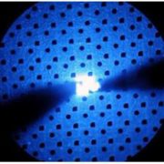
We will offer test reports, please see below an example:
AlGaN template structure report
More products:
GaN Thin Film on Sapphire (Al2O3) Template
You may also like…
-
GaN à base de LED épitaxiales Wafer
PAM-XIAMEN’s GaN(gallium nitride)-based LED epitaxial wafer is for ultra high brightness blue and green light emitting diodes (LED) and laser diodes (LD) application.
-
Ge (germanium) cristaux simples et Wafers
PAM-XIAMEN propose des plaquettes de germanium de 2", 3", 4" et 6", qui est l'abréviation de plaquette Ge cultivée par VGF / LEC. Une plaquette de germanium de type P et N légèrement dopée peut également être utilisée pour l'expérience à effet Hall. À température ambiante, le germanium cristallin est fragile et peu plasticisé. Le germanium a des propriétés semi-conductrices. Le germanium de haute pureté est dopé avec des éléments trivalents (tels que l'indium, le gallium, le bore) pour obtenir des semi-conducteurs en germanium de type P ; et des éléments pentavalents (tels que l'antimoine, l'arsenic et le phosphore) sont dopés pour obtenir des semi-conducteurs en germanium de type N. Le germanium possède de bonnes propriétés semi-conductrices, telles qu'une mobilité élevée des électrons et une mobilité élevée des trous. -
GaN HEMT TRANCHE ÉPITAXIALE
Gallium Nitride (GaN) HEMTs (High Electron Mobility Transistors) are the next generation of RF power transistor technology. Thanks to GaN technology, PAM-XIAMEN now offer AlGaN/GaN HEMT Epi Wafer on sapphire or Silicon, and AlGaN/GaN on sapphire template.
-
Substrat de tranche de SiC
La société dispose d'une ligne complète de production de substrats de plaquettes SiC (carbure de silicium) intégrant la croissance cristalline, le traitement des cristaux, le traitement des plaquettes, le polissage, le nettoyage et les tests. Aujourd'hui, nous fournissons des plaquettes SiC commerciales 4H et 6H avec semi-isolation et conductivité sur axe ou hors axe, tailles disponibles : 5x5 mm2, 10x10 mm2, 2", 3", 4", 6" et 8", perçant des technologies clés telles que comme la suppression des défauts, le traitement des germes de cristal et la croissance rapide, favorisant la recherche et le développement fondamentaux liés à l'épitaxie du carbure de silicium, aux dispositifs, etc.
-
substrat autoportant de GaN
PAM-XIAMEN has established the manufacturing technology for freestanding (gallium nitride)GaN substrate wafer, which is for UHB-LED and LD. Grown by hydride vapour phase epitaxy (HVPE) technology,Our GaN substrate has low defect density.
-
plaquette InAs
PAM-XIAMEN propose des plaquettes de semi-conducteur composé InAs – des plaquettes d'arséniure d'indium qui sont cultivées par LEC (Liquid Encapsulated Czochralski) en tant que qualité épi-prête ou mécanique avec type n, type p ou semi-isolant dans différentes orientations (111) ou (100). De plus, le monocristal InAs présente une mobilité électronique élevée et constitue un matériau idéal pour la fabrication de dispositifs Hall.
-
GaAs tranches épitaxiées
PAM-XIAMEN is manufacturing various types of epi wafer III-V silicon doped n-type semiconductor materials based on Ga, Al, In, As and P grown by MBE or MOCVD. We supply custom GaAs epiwafer structures to meet customer specifications, please contact us for more information.
-
Test Wafer Moniteur Wafer Dummy Wafer
En tant que fabricant de plaquettes factices, PAM-XIAMEN propose des plaquettes factices en silicone / des plaquettes de test / des plaquettes de moniteur, qui sont utilisées dans un dispositif de production pour améliorer la sécurité au début du processus de production et sont utilisées pour le contrôle de livraison et l'évaluation de la forme du processus. Comme les plaquettes de silicium factices sont souvent utilisées à des fins d'expérimentation et de test, leur taille et leur épaisseur sont des facteurs importants dans la plupart des cas. Une plaquette factice de 100 mm, 150 mm, 200 mm ou 300 mm est disponible.