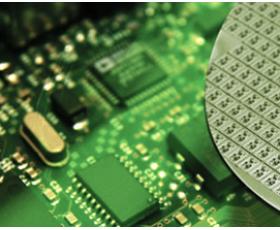


SiC Epitaxy
- Beskrivelse
Beskrivelse
SiC Epitaksi
PAM-XIAMEN provide custom thin film (silicon carbide) SiC epitaxy on 6H or 4H substrates for the development of silicon carbide devices. SiC epi wafer is mainly used for the fabrication of 600V~3300V power devices, including SBD, JBS, PIN, MOSFET, JFET, BJT, GTO, IGBT, etc. With a silicon carbide wafer as a substrate, a chemical vapor deposition (CVD) method is usually used to deposit a layer of single crystal on the wafer to form an epitaxial wafer. Among them, SiC epitaxy are prepared by growing silicon carbide epitaxial layers on conductive silicon carbide substrates, which can be further fabricated into power devices.
1.Specificering af SiC epitaxy:
| Elementer | Specifikation | Typisk værdi |
| Poly-typen | 4H | — |
| Fra orientering mod | 4 deg-off | — |
| <11 2_ 0> | ||
| Ledningsevne | n-type | — |
| dopingmiddel | Kvælstof | — |
| Carrier Koncentration | 5E15-2E18 cm-3 | — |
| Tolerance | ± 25% | ± 15% |
| ensartethed | 2 ”(50,8 mm) <10% | 7% |
| 3 ”(76,2 mm) <20% | 10% | |
| 4 ”(100 mm) <20% | 15% | |
| Tykkelsesområde | 5-15 um | — |
| Tolerance | ± 10% | ± 5% |
| ensartethed | 2 ”<5% | 2% |
| 3 ”<7% | 3% | |
| 4 ”<10% | 5% | |
| Store punktfejl | 2 ”<30 | 2 ”<15 |
| 3 ”<60 | 3 ”<30 | |
| 4 ”<90 | 4 ”<45 | |
| Epi-defekter | ≤20 cm-2 | ≤10 cm-2 |
| Trin Bunching | ≤2,0 nm (Rq) | ≤1,0 nm (Rq) |
| (Ruhed) |
2 mm kantudelukkelse for 50,8 og 76,2 mm, 3 mm kantudelukkelse for 100,0 mmBemærkninger:
• Gennemsnit af alle målepunkter for tykkelse og bærerkoncentration (se s. 5)
• Epi-lag af N-type <20 mikron er forudgående af n-type, 1E18, 0,5 mikron buffertlag
• Ikke alle dopingdensiteter er tilgængelige i alle tykkelser
• Ensartethed: standardafvigelse (σ) / gennemsnit
• Eventuelle særlige krav til epi-parameteren er på anmodning
2. Introduction of SiC Epitaxy
Why do We Need Silicon Carbide Epitaxial Wafer? Because different from the traditional silicon power device manufacturing process, silicon carbide power devices cannot be directly fabricated on silicon carbide single crystal materials. High-quality epitaxial materials must be grown on conductive single crystal substrates, and various devices manufactured on the SiC epitaxial wafer.
The main epitaxial technology for SiC epitaxy growth is chemical vapor deposition (CVD), which realizes a certain thickness and doped silicon carbide epitaxial material through the growth of SiC epitaxy reactor step flow. With the improvement of silicon carbide power device manufacturing requirements and withstand voltage levels, SiC epi wafer continues to develop in the direction of low defects and thick epitaxy.
In recent years, the quality of thin silicon carbide epitaxial materials (<20 μm) has been continuously improved. The microtubule defects in the epitaxial materials have been eliminated. However, the SiC epitaxy defects, such as drop, triangle, carrot, screw dislocation, basal plane dislocation, deep-level defects, etc., become the main factor affecting device performance. With the advancement of SiC epitaxy process, the thickness of the epitaxial layer has developed from a few μm and tens of μm in the past to the current tens of μm and hundreds of μm. Thanks to the advantages of SiC over Si, the SiC epitaxy market is growing rapidly.
Since silicon carbide devices must be fabricated on epitaxial materials, basically all silicon carbide single crystal materials will be used as SiC epitaxial film to grow epitaxial materials. The technology of silicon carbide epitaxial materials has developed rapidly internationally, with the highest epitaxial thickness reaching more than 250 μm. Among them, the epitaxy technology of 20 μm and below has a high maturity. The surface defect density has been reduced to less than 1/cm2, and the dislocation density has been reduced from 105/cm2 to 103/cm2. The dislocation conversion rate of base plane is close to 100%, which has basically met the requirements of epitaxial materials for large-scale production of silicon carbide devices.
In recent years, the international 30 μm~50 μm epitaxial material technology has also matured rapidly, but due to the limitation of SiC epi market demand, the progress of industrialization has been slow. At present, industrialization company can offer silicon carbide epitaxial materials in batches, include Cree SiC epitaxy, PAM-XIAMEN SiC epitaxy, Dow Corning SiC epitaxy etc..
3.Test Methods
No.1. Bærerkoncentration: Nettodoping bestemmes som en gennemsnitsværdi over afer ved hjælp af Hg-sonde CV.
No.2. Tykkelse: Tykkelse bestemmes som en gennemsnitlig værdi over skiven ved hjælp af FTIR.
Nr.3. Størrelsesdefekter: Mikroskopisk inspektion udført ved 100X, på et Olympus optisk mikroskop, eller sammenligneligt.
No.4. Epi-defekter Inspektion eller defektkort udført under KLA-Tencor Candela CS20 Optical Surface Analyzer eller SICA.
No.5. Trinbinding: Trinbinding og ruhed scannes med AFM (atomkraftmikroskop) på et 10μm x 10μm område
3-1:Large Point Defects Descriptions
Defekter, der udviser en klar form for det uassisterede øje og er> 50micron på tværs. Disse funktioner inkluderer pigge, klæbende partikler, chips andcraters. Store punktfejl med mindre end 3 mm fra hinanden tæller som en defekt.
3-2:Epitaxy Defect Descriptions
SiC epitaxy defects include 3C inclusions, comet tails, carrots, particles, silicon droplets and downfall.
4. Application of SiC epitaxial wafer
Effektfaktorkorrektion (PFC)
PV-inverter og UPS (uafbrudt strømforsyning) invertere
Motordrev
Udgangsudligning
Hybride eller elektriske køretøjer
SiC Schottky-diode med 600V, 650V, 1200V, 1700V, 3300V er tilgængelig.
Se nedenfor detaljeret anvendelse efter felt:
| Mark | Radiofrekvens (RF) | Strøm enhed | LED |
| Materiale | SiLDMOS | Si | GaN / Al2O3 |
| GaAs | GAN / Si | GAN / Si | |
| GaN / SiC | SiC / SiC | GaN / SiC | |
| GAN / Si | Ga203 | / | |
| Apparat | SiC-baseret GaN HEMT | SiC-baseret MOSFET SiC-baseret BJT SiC-baseret IGBT SiC-baseret SBD |
/ |
| Ansøgning | Radar, 5G | Elektriske køretøjer | Solid State-belysning |
5. Mechanical wafers with Epi layes: are available, such as for process monitoring, which require wafers with low bow and warpage.
150mm 4H n-type SiC EPI wafers
Intrinsic SiC Epilayer on Silicon carbide substrate
Why do We Need Silicon Carbide Epitaxial Wafer?
SiC MOSFET Structure Homoepitaxial on SiC substrate
Du kan også gerne ...
-
Cz Mono-krystallinsk silicium
PAM-XIAMEN, en monokrystallinsk bulk silicium producent, kan tilbyde <100>, <110> og <111> monokrystallinske silicium wafers med N&P doteringsmiddel i 76,2~200 mm, som dyrkes ved CZ metode. Czochralski-metoden er en krystalvækstmetode, kaldet CZ-metoden. Den er integreret i et varmesystem med lige rør, opvarmet af grafitmodstand, smelter polysilicium indeholdt i en højrent kvartsdigel og indsætter derefter frøkrystallen i overfladen af smelten til svejsning. Derefter sænkes den roterende frøkrystal og smeltes. Kroppen infiltreres og røres, hæves gradvist og afsluttes eller trækkes gennem trinene med halsudskæring, halsudskæring, skulderring, kontrol med samme diameter og efterbehandling.
-
InP wafer
PAM-XIAMEN offers VGF InP(Indium Phosphide) wafer with prime or test grade including low dope, N type or semi-insulating. The mobility of InP wafer is different in different type, low doped one>=3000cm2/V.s, N type>1000 or 2000cm2V.s(depends on different doping concentration), P type: 60+/-10 or 80+/-10cm2/V.s(depends on different Zn doping concentration), and semi-insulting one>2000cm2/V.s, the EPD of Indium Phosphide is below 500/cm2 normally.
-
SIC ansøgning
På grund af SiC fysiske og elektroniske egenskaber, Silicon Carbide baseret enhed er velegnet til korte bølgelængde optoelektroniske, høj temperatur, stråling resistente, og høj effekt / højfrekvente elektroniske enheder, sammenlignet med Si og GaAs anordning -
Fritstående GaN-substrat
PAM-XIAMEN har etableret den fremstillingsteknologi til fritstående (galliumnitrid) GaN substratwafer, der er til UHB-LED og LD. Vokset med hydrid dampfase epitaxy (HVPE) teknologi, Vores GaN substrat har lav defekt tæthed.
-
SiC Wafer Substrat
The company has a complete SiC(silicon carbide) wafer substrate production line integrating crystal growth, crystal processing, wafer processing, polishing, cleaning and testing. Nowadays we supply commercial 4H and 6H SiC wafers with semi insulation and conductivity in on-axis or off-axis, available size:5x5mm2,10x10mm2, 2”,3”,4”, 6” and 8″, breaking through key technologies such as defect suppression, seed crystal processing and rapid growth, promoting basic research and development related to silicon carbide epitaxy, devices, etc.
-
GaAs Epiwafer
PAM-XIAMEN fremstiller forskellige typer epi wafer III-V siliciumdoteret n-type halvledermaterialer baseret på Ga, Al, In, As og P dyrket af MBE eller MOCVD. Vi leverer tilpassede GaAs epiwafer-strukturer for at opfylde kundernes specifikationer, kontakt os venligst for mere information.
-
Ge (Germanium) enkelte krystaller og Wafers
PAM-XIAMEN tilbyder 2”, 3”, 4” og 6” germanium wafer, som er en forkortelse for Ge wafer dyrket af VGF / LEC. Let dopet Germanium wafer af P og N type kan også bruges til Hall effekt eksperiment. Ved stuetemperatur er krystallinsk germanium skørt og har ringe plasticitet. Germanium har halvlederegenskaber. Germanium med høj renhed er dopet med trivalente grundstoffer (såsom indium, gallium, bor) for at opnå P-type germanium-halvledere; og pentavalente grundstoffer (såsom antimon, arsen og phosphor) er dopet for at opnå N-type germanium-halvledere. Germanium har gode halvlederegenskaber, såsom høj elektronmobilitet og høj hulmobilitet. -
SiC Wafer Reclaim
PAM-XIAMEN er i stand til at tilbyde følgende SiC genvinde wafer-tjenester.