كربيد إبيتاز
- وصف
وصف المنتج
كربيد إبيتاز
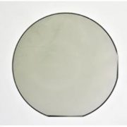
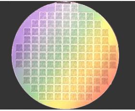
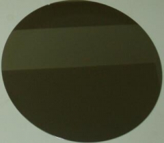
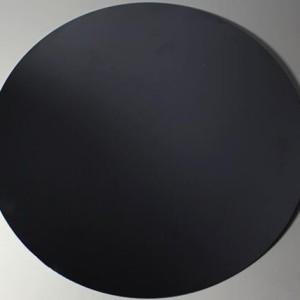
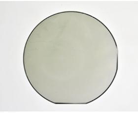
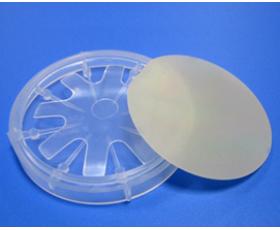
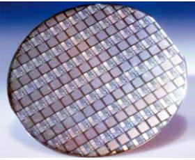
PAM-XIAMEN provide custom thin film (silicon carbide) SiC epitaxy on 6H or 4H substrates for the development of silicon carbide devices. SiC epi wafer is mainly used for the fabrication of 600V~3300V power devices, including SBD, JBS, PIN, MOSFET, JFET, BJT, GTO, IGBT, etc. With a silicon carbide wafer as a substrate, a chemical vapor deposition (CVD) method is usually used to deposit a layer of single crystal on the wafer to form an epitaxial wafer. Among them, SiC epitaxy are prepared by growing silicon carbide epitaxial layers on conductive silicon carbide substrates, which can be further fabricated into power devices.
1.Specification of SiC epitaxy:
| البنود | مواصفات | القيمة النموذجية |
| بولي نوع | 4H | — |
| إيقاف التوجه نحو | 4 درجة قبالة | — |
| <11 2_ 0> | ||
| الموصلية | نوع ن | — |
| المقوي | نتروجين | — |
| الناقل تركيز | 5E15-2E18 cm-3 | — |
| تفاوت | ± 25٪ | ± 15٪ |
| انتظام | 2 "(50.8mm) <10٪ | 7٪ |
| 3 "(76.2mm) <20٪ | 10٪ | |
| 4 "(100MM) <20٪ | 15٪ | |
| المدى سمك | 5-15 ميكرون | — |
| تفاوت | ± 10٪ | ± 5٪ |
| انتظام | 2 "<5٪ | 2٪ |
| 3 "<7٪ | 3٪ | |
| 4 "<10٪ | 5٪ | |
| العيوب نقطة كبيرة | 2 "<30 | 2 "<15 |
| 3 "<60 | 3 "<30 | |
| 4 "<90 | 4 "<45 | |
| عيوب برنامج التحصين الموسع | ≤20 cm-2 | ≤10 cm-2 |
| خطوة Bunching | ≤2.0nm (RQ) | ≤1.0nm (RQ) |
| (خشونة) |
2 mm edge exclusion for 50.8 and 76.2 mm, 3 mm edge exclusion for 100.0 mmNotes:
• Average of all measurement points for thickness and carrier concentration (see pg. 5)
• N-type epi layers <20 microns are preceeded by n-type, 1E18, 0.5 micron buffer layer
• Not all doping densities are available in all thicknesses
• Uniformity:standard deviation(σ)/average
• Any special requirement on the epi-parameter is on request
2. Introduction of SiC Epitaxy
Why do We Need Silicon Carbide Epitaxial Wafer? Because different from the traditional silicon power device manufacturing process, silicon carbide power devices cannot be directly fabricated on silicon carbide single crystal materials. High-quality epitaxial materials must be grown on conductive single crystal substrates, and various devices manufactured on the SiC epitaxial wafer.
The main epitaxial technology for SiC epitaxy growth is chemical vapor deposition (CVD), which realizes a certain thickness and doped silicon carbide epitaxial material through the growth of SiC epitaxy reactor step flow. With the improvement of silicon carbide power device manufacturing requirements and withstand voltage levels, SiC epi wafer continues to develop in the direction of low defects and thick epitaxy.
In recent years, the quality of thin silicon carbide epitaxial materials (<20 μm) has been continuously improved. The microtubule defects in the epitaxial materials have been eliminated. However, the SiC epitaxy defects, such as drop, triangle, carrot, screw dislocation, basal plane dislocation, deep-level defects, etc., become the main factor affecting device performance. With the advancement of SiC epitaxy process, the thickness of the epitaxial layer has developed from a few μm and tens of μm in the past to the current tens of μm and hundreds of μm. Thanks to the advantages of SiC over Si, the SiC epitaxy market is growing rapidly.
Since silicon carbide devices must be fabricated on epitaxial materials, basically all silicon carbide single crystal materials will be used as SiC epitaxial film to grow epitaxial materials. The technology of silicon carbide epitaxial materials has developed rapidly internationally, with the highest epitaxial thickness reaching more than 250 μm. Among them, the epitaxy technology of 20 μm and below has a high maturity. The surface defect density has been reduced to less than 1/cm2, and the dislocation density has been reduced from 105/cm2 to 103/cm2. The dislocation conversion rate of base plane is close to 100%, which has basically met the requirements of epitaxial materials for large-scale production of silicon carbide devices.
In recent years, the international 30 μm~50 μm epitaxial material technology has also matured rapidly, but due to the limitation of SiC epi market demand, the progress of industrialization has been slow. At present, industrialization company can offer silicon carbide epitaxial materials in batches, include Cree SiC epitaxy, PAM-XIAMEN SiC epitaxy, Dow Corning SiC epitaxy etc..
3.Test Methods
NO.1. تركيز الناقل: يتم تحديد صافي المنشطات باعتبارها متوسط قيمة عبر عفر باستخدام الزئبق التحقيق CV.
NO.2. يتم تحديد سمك كقيمة متوسط عبر الرقاقة باستخدام FTIR: سمك.
عيوب نقطة No.3.Large: التفتيش المجهري أجريت في 100X، على أوليمبوس البصرية مجهر، أو قابلة للمقارنة.
No.4. Epi Defects Inspection or defect map performed under KLA-Tencor Candela CS20 Optical Surface Analyzer or SICA.
رقم 5. خطوة bunching: bunching خطوة والخشونة وscaned التي كتبها AFM (القوة الذرية المجهر) على مساحة x10μm 10μm
3-1:Large Point Defects Descriptions
العيوب التي تظهر في شكل واضح للعين بدون مساعدة وهي> 50microns عبر. وتشمل هذه الميزات المسامير، جسيمات الملتصقة، ورقائق andcraters. عيوب نقطة كبيرة أقل من 3 مم حساب بعضها البعض مثل عيب واحد.
3-2:Epitaxy Defect Descriptions
SiC epitaxy defects include 3C inclusions, comet tails, carrots, particles, silicon droplets and downfall.
4. Application of SiC epitaxial wafer
تصحيح معامل القدرة (PFC)
العاكس PV وUPS (إمدادات الطاقة غير المنقطعة) العاكسون
محركات السيارات
الإخراج تصحيح
هجين أو السيارات الكهربائية
كربيد شوتكي الصمام الثنائي مع 600V، 650V، 1200V، 1700V، 3300V هو متاح.
Please see below detail application by field:
| Field | Radio Frequency(RF) | Power Device | LED |
| مادة | SiLDMOS | سي | GaN/Al2O3 |
| GaAs | GaN/Si | GaN/Si | |
| GaN/SiC | SiC/SiC | GaN/SiC | |
| GaN/Si | Ga203 | / | |
| Device | SiC based GaN HEMT | SiC based MOSFET SiC based BJT SiC based IGBT SiC based SBD |
/ |
| Application | Radar, 5G | Electric vehicles | Solid State Lighting |
5. Mechanical wafers with Epi layes: are available, such as for process monitoring, which require wafers with low bow and warpage.
150mm 4H n-type SiC EPI wafers
Intrinsic SiC Epilayer on Silicon carbide substrate
Why do We Need Silicon Carbide Epitaxial Wafer?
هيكل SiC MOSFET متجانس على الركيزة SiC

