PAM-XIAMEN tilbyder galliumnitrid wafersubstrat for UHB-LED, galliumnitrid wafer, LD og andre halvlederkomponenter.

SiC Wafer
Silicon Carbideï¼SiC) Vafler PAM-XIAMENÂ tilbud Silicon Carbide crytal vafler og epitaksi, som bruges til optisk udstyr, High Power Devices, høj temperatur Enheder, High Frequency Power Devices
GaAs Wafer
PAM-XIAMEN tilbyder Galliumarsenid wafersubstrat og epitaxi til LED, LD og Mikroelektronik applikationer

Germanium Wafer
PWAMÂ tilbud halvledermaterialer, (Ge) Germanium enkelte krystaller og Vafler vokset med VGF / LEC
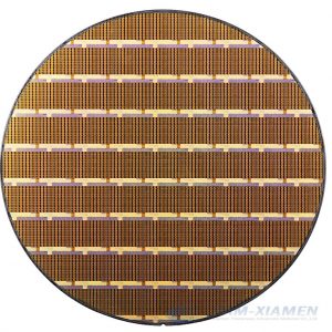
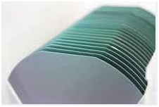
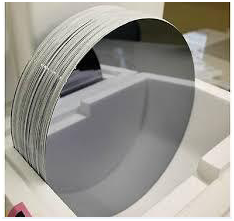
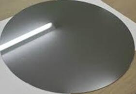
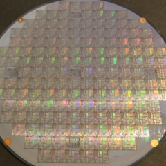
Silicon Wafer
PAM-XIAMEN, et siliciumwafer-fremstillingsfirma, tilbyder siliciumwafer: FZ Siliciumwafer, Test Wafer Monitor Wafer Dummy Wafer, Test Wafer, CZ wafer, epitaksial wafer, poleret wafer, ætsningswafer.
Fremstillingsprocessen for siliciumwafer er krystaltrækning, siliciumwaferslibning, siliciumwaferslibning, affasning, ætsning, polering, rengøring og inspektion, blandt hvilke krystaltrækning, siliciumwafer-polering og -inspektion er kerneleddet i siliciumwafer-fremstilling. Som det grundlæggende halvledersubstrat skal siliciumwafers have høje standarder for renhed, overfladeplanhed, renhed og urenhedsforurening for at bevare chippens oprindeligt designede funktioner. De høje specifikationskrav til halvledersiliciumwafers gør fremstillingsprocessen kompliceret. De fire kernetrin omfatter polysiliciumoprensning og polysiliciumstøbning, enkeltkrystal siliciumwafervækst og siliciumwaferskæring og -formning. Som råmateriale til wafer fab bestemmer kvaliteten af silicium wafers direkte stabiliteten af silicium wafer påføringsprocessen. Siliciumwafere i store størrelser er blevet den fremtidige udviklingstrend for siliciumwafers. For at forbedre produktionseffektiviteten og reducere omkostningerne bruges flere og flere store siliciumwafers.

Wafer FABRIKATIONS
PAM-XIAMEN Tilbud fotoresist plade med fotoresist og fotomaske, og give nanolithography (fotolitografi): Overfladebehandling, Fotoresist gælder, Soft bage, Justering, Eksponering, udvikling, Hård bage, Develop inspicere, Etch, Fotoresist fjernelse (strimmel), Endelig inspektion.
-
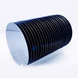
12 "Prime Grade Silicon Wafer
PAM-XIAMEN tilbyder 300 mm blottede siliciumwafers (12 tommer) i førsteklasses kvalitet, n-type eller p-type, og tykkelsen på 300 mm siliciumwafer er 775±15. Sammenlignet med andre leverandører af siliciumwafer er Powerway Wafers pris på siliciumwafer mere konkurrencedygtig med højere kvalitet. 300 mm silicium wafers har et højere udbytte pr. wafer end gennemtrængelige silicium wafers med stor diameter.
-
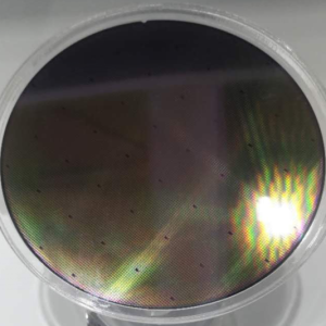
12 "Silicon Wafers 300mm TOX (Si Thermal Oxidation Wafer)
PAM-XIAMEN tilbyder 300 mm siliciumoxid wafer og dioxid wafer. Termisk oxid silicium wafer eller silicium dioxid wafer er en bar silicium wafer med oxidlag dyrket ved tør eller våd oxidationsproces. Det termiske oxidlag af siliciumwaferen dyrkes normalt i en vandret rørovn, og temperaturområdet for siliciumwaferoxid er generelt 900 ℃ ~ 1200 ℃. Sammenlignet med CVD-oxidlag har siliciumwaferoxidlag højere ensartethed, bedre kompaktitet, højere dielektrisk styrke og bedre kvalitet.
-
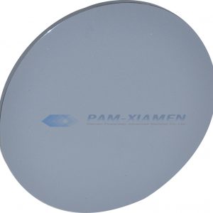
12 "Test Grade Silicon Wafer
PAM-XIAMEN tilbyder 300 mm bare silicium wafers (12 tommer) dummy, testkvalitet, n type eller p type. Sammenlignet med andre leverandører af siliciumwafer tilbyder Powerway Wafer professionel service til konkurrencedygtige priser.
-
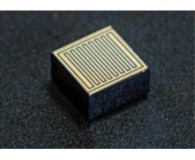
Epi Wafer til Laser Diode
GaAs-baseret LD-epitaksi-wafer, som kan generere stimulerende emission, bruges i vid udstrækning til fremstilling af laserdioder, da de overlegne GaAs-epitaksiale waferegenskaber gør enheden til et lavt energiforbrug, høj effektivitet, lang levetid osv. Ud over galliumarsenid LD epi-wafer , almindeligt anvendte halvledermaterialer er cadmiumsulfid (CdS), indiumphosphid (InP) og zinksulfid (ZnS).
-
Float-Zone Mono-krystallinsk silicium
PAM-XIAMEN kan tilbyde float zone silicium wafer, som opnås ved Float Zone metoden. Monokrystallinske siliciumstænger føres gennem floatzonevækst, og forarbejde derefter de monokrystallinske siliciumstænger til siliciumwafers, kaldet floatzone siliciumwafers. Da den zonesmeltede siliciumwafer ikke er i kontakt med kvartsdigelen under den flydende zone siliciumproces, er siliciummaterialet i en suspenderet tilstand. Derved er det mindre forurenet under processen med flydende zonesmeltning af silicium. Kulstofindholdet og oxygenindholdet er lavere, urenhederne er mindre, og resistiviteten er højere. Den er velegnet til fremstilling af strømudstyr og visse elektroniske højspændingsenheder.
-
Wafer Støberi Services
PAM-XIAMEN leverer wafer-støberitjenester med avanceret halvlederprocesteknologi og drager fordel af vores upstream-erfaringer med substrat- og wafer-ekspaxi,
PAM-XIAMEN skal være den mest avancerede waferteknologi og støberitjenester for fabelløse virksomheder, IDM'er og forskere.
-
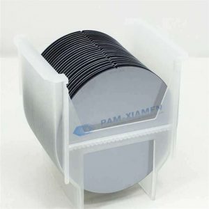
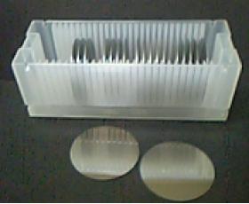
Test Wafer Monitor Wafer Dummy Wafer
Som producent af dummy wafer tilbyder PAM-XIAMEN silikone dummy wafer / test wafer / monitor wafer, som bruges i en produktionsenhed for at forbedre sikkerheden i begyndelsen af produktionsprocessen og bruges til leveringskontrol og evaluering af procesform. Da dummy silicium wafers ofte bruges til eksperimenter og test, er størrelse og tykkelse deraf vigtige faktorer i de fleste tilfælde. 100 mm, 150 mm, 200 mm eller 300 mm dummy wafer er tilgængelig.
-
Cz Mono-krystallinsk silicium
PAM-XIAMEN, en monokrystallinsk bulk silicium producent, kan tilbyde <100>, <110> og <111> monokrystallinske silicium wafers med N&P doteringsmiddel i 76,2~200 mm, som dyrkes ved CZ metode. Czochralski-metoden er en krystalvækstmetode, kaldet CZ-metoden. Det er integreret i et varmesystem med lige rør, opvarmet af grafitmodstand, smelter polysilicium indeholdt i en højrent kvartsdigel og indsætter derefter frøkrystallen i overfladen af smelten til svejsning. Derefter sænkes den roterende frøkrystal og smeltes. Kroppen infiltreres og røres, hæves gradvist og afsluttes eller trækkes gennem trinene med halsudskæring, halsudskæring, skulderring, kontrol med samme diameter og efterbehandling.
-
Epitaksial Silicon Wafer
Silicon Epitaxial Wafer (Epi Wafer) er et lag af epitaksial silicium enkeltkrystal aflejret på en enkeltkrystal siliciumwafer (bemærk: det er tilgængeligt til at dyrke et lag polykrystallinsk siliciumlag oven på en højtdoteret enkeltkrystallinsk siliciumwafer, men det behov bufferlag (såsom oxid eller poly-Si) i mellem bulk Si substrat og det øverste epitaksiale silicium lag.Det kan også bruges til tynd film transistor.
-
Poleret Wafer
PAM-XIAMEN kan tilbyde poleret wafer, n type eller p type med orientering på <100>, <110> eller <111>. FZ polerede wafere, hovedsageligt til produktion af silicium ensretter (SR), silicium kontrolleret ensretter (SCR), Giant Transistor (GTR), tyristor (GRO)
-
ætsning Wafer
De ætsende siliciumskiver, der tilbydes af PAM-XIAMEN, er N-type eller P-type ætseskiver, som har lav ruhed, lav reflektivitet og høj reflektivitet. Ætsewaferen har egenskaberne lav ruhed, god glans og relativt lave omkostninger og erstatter direkte den polerede wafer eller epitaksiale wafer, som har relativt høje omkostninger til at fremstille de elektroniske elementer på nogle områder, hvilket reducerer omkostningerne.
-
Nanofabrikationsfotoresist
PAM-XIAMEN Tilbud fotoresist plade med fotoresist