

SiCのエピタキシー
- 説明
製品の説明
SiCのエピタキシー
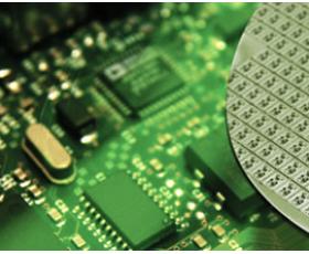
PAM-XIAMEN provide custom thin film (silicon carbide) SiC epitaxy on 6H or 4H substrates for the development of silicon carbide devices. SiC epi wafer is mainly used for the fabrication of 600V~3300V power devices, including SBD, JBS, PIN, MOSFET, JFET, BJT, GTO, IGBT, etc. With a silicon carbide wafer as a substrate, a chemical vapor deposition (CVD) method is usually used to deposit a layer of single crystal on the wafer to form an epitaxial wafer. Among them, SiC epitaxy are prepared by growing silicon carbide epitaxial layers on conductive silicon carbide substrates, which can be further fabricated into power devices.
1.SiCエピタキシーの仕様:
| アイテム | 仕様 | 標準値 |
| ポリタイプ | 4H | — |
| オフの方向に向けて | 4度オフ | — |
| <11 2_ 0> | ||
| 導電率 | n型 | — |
| ドーパント | 窒素 | — |
| キャリア濃度 | 5E15-2E18 cm-3 | — |
| 公差 | ±25% | ±15% |
| 均一 | 2” (50.8ミリメートル)<10% | 7% |
| 3” (76.2ミリメートル)<20% | 10% | |
| 4” (100ミリメートル)<20% | 15% | |
| 厚さの範囲 | 5-15ミクロン | — |
| 公差 | ±10% | ±5% |
| 均一 | 2” <5% | 2% |
| 3” <7% | 3% | |
| 4” <10% | 5% | |
| 大きな点欠陥 | 2” <30 | 2” <15 |
| 3” <60 | 3” <30 | |
| 4” <90 | 4” <45 | |
| エピ欠陥 | ≤20cm-2 | ≤10cm-2 |
| ステップバンチング | ≤2.0nmさ(Rq) | ≤1.0nmさ(Rq) |
| (粗さ) |
50.8および76.2mmの場合は2mmのエッジ除外、100.0mmの場合は3mmのエッジ除外注:
•厚さとキャリア濃度のすべての測定ポイントの平均(5ページを参照)
•20ミクロン未満のN型エピ層の前には、n型、1E18、0.5ミクロンのバッファー層があります。
•すべてのドーピング密度がすべての厚さで利用できるわけではありません
•均一性:標準偏差(σ)/平均
•エピパラメータに関する特別な要件はリクエストに応じて提供されます
2. Introduction of SiC Epitaxy
なぜ炭化ケイ素エピタキシャルウェーハが必要なのですか? Because different from the traditional silicon power device manufacturing process, silicon carbide power devices cannot be directly fabricated on silicon carbide single crystal materials. High-quality epitaxial materials must be grown on conductive single crystal substrates, and various devices manufactured on the SiC epitaxial wafer.
The main epitaxial technology for SiC epitaxy growth is chemical vapor deposition (CVD), which realizes a certain thickness and doped silicon carbide epitaxial material through the growth of SiC epitaxy reactor step flow. With the improvement of silicon carbide power device manufacturing requirements and withstand voltage levels, SiC epi wafer continues to develop in the direction of low defects and thick epitaxy.
In recent years, the quality of thin silicon carbide epitaxial materials (<20 μm) has been continuously improved. The microtubule defects in the epitaxial materials have been eliminated. However, the SiC epitaxy defects, such as drop, triangle, carrot, screw dislocation, basal plane dislocation, deep-level defects, etc., become the main factor affecting device performance. With the advancement of SiC epitaxy process, the thickness of the epitaxial layer has developed from a few μm and tens of μm in the past to the current tens of μm and hundreds of μm. Thanks to the advantages of SiC over Si, the SiC epitaxy market is growing rapidly.
Since silicon carbide devices must be fabricated on epitaxial materials, basically all silicon carbide single crystal materials will be used as SiC epitaxial film to grow epitaxial materials. The technology of silicon carbide epitaxial materials has developed rapidly internationally, with the highest epitaxial thickness reaching more than 250 μm. Among them, the epitaxy technology of 20 μm and below has a high maturity. The surface defect density has been reduced to less than 1/cm2, and the dislocation density has been reduced from 105/cm2 to 103/cm2. The dislocation conversion rate of base plane is close to 100%, which has basically met the requirements of epitaxial materials for large-scale production of silicon carbide devices.
In recent years, the international 30 μm~50 μm epitaxial material technology has also matured rapidly, but due to the limitation of SiC epi market demand, the progress of industrialization has been slow. At present, industrialization company can offer silicon carbide epitaxial materials in batches, include Cree SiC epitaxy, PAM-XIAMEN SiC epitaxy, Dow Corning SiC epitaxy etc..
3.Test Methods
1番。 キャリア濃度ネットドーピングを水銀プローブCVを用いてのafer全体の平均値として決定されます。
第2号。 厚さ:厚さは、FTIRを用いてウエハ全体の平均値として決定されます。
No.3.Large点欠陥:顕微鏡検査は、オリンパス光学顕微鏡で、100倍で行われ、または同等の。
No.4。 Epi DefectsInspectionまたはKLA-TencorCandela CS20 Optical SurfaceAnalyzerまたはSICAで実行される欠陥マップ。
第5号。 ステップバンチング:ステップバンチングと粗さは10μMのx10μm領域にAFM(原子間力顕微鏡)によってscanedれます
3-1:Large Point Defects Descriptions
肉眼に明確な形状を示し、ある欠陥>全体50microns。 これらの機能は、スパイク、付着粒子、チップandcratersが含まれます。 大きい点欠陥3mm未満で離れつの欠陥としてカウント。
3-2:Epitaxy Defect Descriptions
SiC epitaxy defects include 3C inclusions, comet tails, carrots, particles, silicon droplets and downfall.
4. Application of SiC epitaxial wafer
力率補正(PFC)
PVインバータやUPS(無停電電源装置)インバータ
モータードライブ
出力整流
ハイブリッドや電気自動車
600V、650V、1200V、1700V、3300VとSiCショットキー・ダイオードが使用可能です。
以下の分野別の詳細アプリケーションをご覧ください。
| フィールド | 無線周波数(RF) | パワーデバイス | LED |
| 材料 | SiLDMOS | シ | GaN / Al2O3 |
| GaAsの | GaN / Si | GaN / Si | |
| GaN / SiC | SiC / SiC | GaN / SiC | |
| GaN / Si | Ga203 | / | |
| デバイス | SiCベースのGaN HEMT | SiCベースのMOSFET SiCベースのBJT SiCベースのIGBT SiCベースのSBD |
/ |
| アプリケーション | レーダー、5G | 電気自動車 | ソリッドステート照明 |
5. Mechanical wafers with Epi layes: are available, such as for process monitoring, which require wafers with low bow and warpage.
Intrinsic SiC Epilayer on Silicon carbide substrate
あなたも好きかも...
-
ゲルマニウム(ゲルマニウム)単結晶とウェーハ
PAM-XIAMEN は、2 インチ、3 インチ、4 インチ、および 6 インチのゲルマニウム ウェーハを提供しています。これは、VGF / LEC によって成長させた Ge ウェーハの略です。 低濃度ドープの P 型および N 型ゲルマニウム ウェーハは、ホール効果の実験にも使用できます。 結晶ゲルマニウムは室温では脆く、可塑性がほとんどありません。 ゲルマニウムは半導体の性質を持っています。 高純度ゲルマニウムに三価元素(インジウム、ガリウム、ホウ素など)をドープすると、P 型ゲルマニウム半導体が得られます。 5価元素(アンチモン、ヒ素、リンなど)をドープしてN型ゲルマニウム半導体を得る。 ゲルマニウムは、高い電子移動度や高い正孔移動度など、優れた半導体特性を備えています。 -
GaAsのエピウェーハ
PAM-XIAMEN は、MBE または MOCVD によって成長させた、Ga、Al、In、As、P をベースとしたさまざまな種類のエピ ウェハ III-V シリコンドープ n 型半導体材料を製造しています。 当社では、お客様の仕様を満たすカスタム GaAs エピウェーハ構造を提供しています。詳細については、お問い合わせください。
-
自立GaN基板
PAM-アモイUHB-LEDおよびLDのためのものである(窒化ガリウム)GaN基板ウエハを、自立するための製造技術を確立しました。 ハイドライド気相エピタキシー(HVPE)技術によって成長させ、我々のGaN基板は、低欠陥密度を有します。
-
InP基板
PAM-XIAMEN は、低ドープ、N タイプ、または半絶縁性を含むプライムまたはテストグレードの VGF InP (リン化インジウム) ウェーハを提供しています。 InPウェハの移動度はタイプによって異なり、低ドープのもの>=3000cm2/Vs、Nタイプ>1000または2000cm2V.s(異なるドーピング濃度に依存)、Pタイプ:60+/-10または80+/-10cm2 /Vs(異なるZnドーピング濃度に依存)、半絶縁性のもの>2000cm2/Vs、リン化インジウムのEPDは通常500/cm2未満です。
-
SiCウェハ基板
同社は、結晶成長、結晶処理、ウェーハ処理、研磨、洗浄、テストを統合した完全なSiC(炭化ケイ素)ウェーハ基板生産ラインを持っています。 現在、当社は、オンアクシスまたはオフアクシスで半絶縁性と導電性を備えた市販の 4H および 6H SiC ウェハーを供給しています。利用可能なサイズは 5x5mm2、10x10mm2、2 インチ、3 インチ、4 インチ、6 インチ、8 インチであり、次のような主要技術を突破しています。欠陥抑制、種結晶加工、高速成長など、炭化珪素エピタキシー、デバイス等に関する基礎研究開発を推進します。
-
CZ単結晶シリコン
単結晶バルクシリコン生産会社である PAM-XIAMEN は、CZ 法で成長した、N&P ドーパントを含む 76.2 ~ 200 mm の <100>、<110>、および <111> 単結晶シリコン ウェーハを提供できます。 チョクラルスキー法とは、CZ法と呼ばれる結晶成長法の一つである。 直管加熱システムに組み込まれており、黒鉛抵抗によって加熱され、高純度石英るつぼに入ったポリシリコンを溶解し、その融液の表面に種結晶を挿入して溶接します。 その後、回転している種結晶を下降させて溶かします。 ボディを浸し、触り、徐々に引き上げ、ネッキング、ネッキング、ショルダリング、等径管理、仕上げの工程を経て仕上げまたは引き抜きを行います。
-
SiCウェハ取り戻します
PAM-厦門は、ウェハのサービスを再利用し、次のSiCを提供することができます。
-
SICアプリケーション
SiCの物理的および電子的特性のために、炭化ケイ素ベースのデバイスは、Si及びGaAsデバイスに比べて、短い波長の光電子、高温、耐放射線性、高出力/高周波電子機器によく適しています