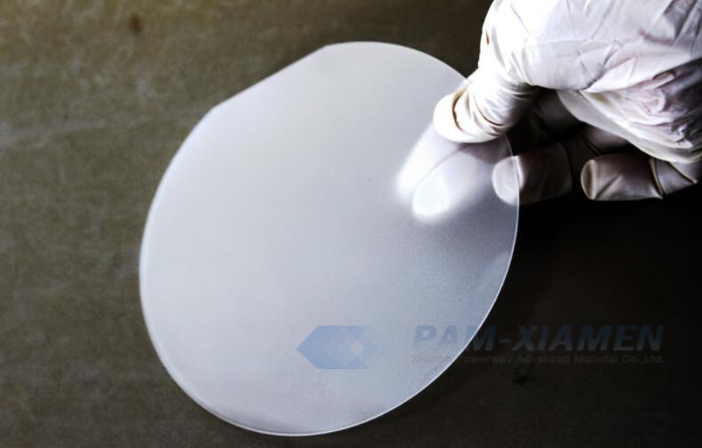
PAM-XIAMEN can offer LED epitaxy wafers and is able to offer GaN foundry services & supplies for LEDs. The GaN foundry services include OEM growth service, COW process and various test services. Specifically as follows:
1. OEM Service – Customized AlGaN-based Thin Film Epi Structure
We supply 2, 4 inch DUV-LED epitaxial wafer custom serve. And the wavelength of the GaN epitaxial wafer from our GaN foundry is from 265nm to 280nm.
In addition, custom serve of 2&4 inch AlGaN based epitaxial LED structures is available. Therein, the Al composition of AlGaN epi layer is adjustable among 0~100%
2. GaN Chip Foundry Services – COW Process for Blue, UVA and UVC LED Devices
GaN services: COW process and single OEM service in our foundry for blue, UVA and UVC LED devices are including photolithography, reactive ion etching (for GaN, AlN and AlGaN), reactive ion etching (SiO2, Si3N4), PECVD (SiO2, Si3N4), electron beam evaporation (Au, Ni, Cr, Al, Ti), electron beam evaporation (ITO), rapid annealing, CMP (thinning, grinding, polishing) and etc.
2.1 Photolithography for GaN LED
We can perform 1μm precision photolithography for GaN LED wafers of 4 inches and below, which can be precisely controlled according to customer needs.
2.2 Inductively Coupled Plasma Etching (ICP) for GaN based LED Epi
We are able to perform pattern etching for GaN, AlN and AlGaN materials.
2.3 Reactive Ion Etching (RIE) for GaN Semiconductor Wafer
For SiO2 and SiNx thin films, pattern etching is performed on GaN wafers.
2.4 Plasma Enhanced Chemical Vapor Deposition (PECVD) for GaN Epiwafers
For Wafers 6 inches and below, plasma-enhanced chemical vapor deposition is performed to form a uniform, dense, and thickness-controllable SiO2 or SiNx film on the surface of GaN epitaxy.
2.5 Electron beam evaporation coating (E-Beam) on GaN Epitaxial Wafer
By bombarding the target with electron beams from an electron gun, ITO thin film evaporation is carried out on the GaN surface, the material are Au, Ni, Cr, Al, Ti and so on
Vapor deposition of metal thin films such as Ag and Pt.
2.6 Rapid Annealing (RTA) of GaN Thin Film
Based on your process requirements, our rapid annealing can use different gases such as N2 and O2 to match different process, and set different heating and cooling rates, annealing temperatures, and annealing times to alloy and fuse the metal electrodes to meet the electrical requirements of the product.
3. GaN Test Service
We supply test services for GaN wafers as below:
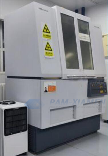
3.1 XRD Test of Semiconductor Thin Film Materials
ω-scan of different crystal planes of 2-4 inch semiconductor thin film materials: the rocking curve test can use the inverted space imaging principle to realize the inverted space Mapping measurement, obtain the composition and stress of the ternary alloy materials such as AlGaN, and also have the functions of film thickness measurement.
3.2 AFM Test for Epiwafers
AFM test has two modes: Tapping and Contact, which can detect the surface topography of materials, equipped with a C-AFM module capable of probing current channels in materials. Using the KPFM function, the work function of metal materials and the surface potential of semiconductor materials can be tested. Using the LFM function, the friction force of the micro-domains on the surface of organic materials can be tested. Using MFM, the magnetic domain distribution of the sample can be measured.
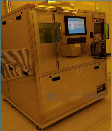
3.3 Epitaxial Wafer PL Spectrum Scanning Imager
Epitaxial wafer PL spectrum scanning imager can be compatible under 6 inches Epitaxial wafer, the test content includes: blue LED epitaxial wafer peak wavelength (WLP), dominant wavelength (WLD), spectral half-width (HW), integrated light intensity (INT), peak intensity (PI); epitaxial film thickness and reflectivity (PR); display and output the average value of each measured parameter (Mean), mean square error (Std), standard deviation rate (CV) and other statistical results, and graphically display the mapping distribution of each parameter; measure the warpage of epitaxial wafers.
3.4 Kelvin Probe Force Microscope
The atomic force microscope has the KPFM test function, which can test the work function of metal materials and the surface potential of semiconductor materials.
At the same time, a light-assisted test system can be installed to test the changes in the surface potential of semiconductor devices under illumination conditions.
3.5 High and Low Temperature Hall Effect Test
We provide high temperature Hall measurement of semiconductor thin film materials, the test temperature is 90-700K, and the magnetic field strength of the magnet is 0.5 T, the maximum measured sheet resistance is 10^11 ohm/sq, the minimum test current is 1μA, the DC range is from 1μA to 20 mA, and AC mode is also available (high resistance samples cannot be measured in AC mode).
3.6 Deep Level Transient Spectrum
High-temperature deep-level transient spectroscopy and light-assisted deep-level transient spectroscopy testing is provided to detect semiconductors Deep energy levels and interface states of medium and trace impurities and defects. The deep level transient spectrum can be given to characterize the semiconductor band gap The DLTS spectra of impurities, deep defect levels and interface states within the distribution with temperature (i.e. energy).
3.7 Quantum Transport Test
We provide low temperature and strong magnetic field quantum transport test, Line magnetoresistance test and Hall test. Usually the samples are First measure the variable temperature IV, and then measure the magnetoresistance. Magnetoresistive measuring range is 0.1ohm-100ohm.
For III-V semiconductors, low Temperature and strong magnetic field Hall test can obtain sample mobility and electron concentration changes with temperature. For quantity samples of sub-confinement effects such as two-dimensional electron gas, low warm and strong magnetic fields can lead to Zeeman splitting, thereby quantum effects such as SdH oscillations are observed, and transport properties of different sub bands (mobility electron concentration Spend) can be obtained.
3.8 Analysis of Electrical Parameters of Semiconductor Thin Film Materials and Structures
Provides electrical parameter analysis of semiconductor thin film materials and structures, DC Source measurement unit indicators: maximum voltage 210V, maximum current 100mA, maximum power 2W; pulse measurement unit indicators: system pulse generator frequency: 50MHz-1Hz; minimum pulse width: 10ns; maximum pulse voltage: 80V, -40V-40V.
3.9 Tip Enhanced Raman Spectrometer
Provides micro-area Raman testing, owns Neaspec tip-enhanced Raman spectrometer (TERS), with a spatial resolution of 10nm, and increased Raman intensity.
It is more than 1000 times stronger, and can measure the near field strength and bit confidence of the third order or more.
3.10 Optical Test
The optical test platform has 213, 266, 325, 532 and 633nm lasers and can be used to measure materials with different emission wavelengths. The spectrometer adopts iHR550 equipment, the resolution reaches 0.33nm, and the collection wavelength range covers ultraviolet, visible and infrared parts
Opitcal test can measure bulk materials and micron-sized samples. The platform spectroscopic device is non-integrated and can freely combine components with different functions to meet various test requirements, such as measurement of optical polarization, pressure spectroscopy, low temperature and variable power. Provide time-resolved spectral testing of semiconductor thin film materials and structures. By recording the changes in the spectrum over time, we can understand the events and processes that occur in the instantaneous process, so as to obtain information that cannot be obtained in the steady-state spectrum (integrated spectrum). The measurement of the carrier radiation lifetime is used to obtain relevant information such as the lifetime of the excited state, transition probability, collision cross section, reaction rate and energy transfer.
Remark:
The Chinese government has announced new limits on the exportation of Gallium materials (such as GaAs, GaN, Ga2O3, GaP, InGaAs, and GaSb) and Germanium materials used to make semiconductor chips. Starting from August 1, 2023, exporting these materials is only allowed if we obtains a license from the Chinese Ministry of Commerce. Hope for your understanding and cooperation!

لمزيد من المعلومات، يرجى الاتصال بنا على البريد الإلكترونيvictorchan@powerwaywafer.com و powerwaymaterial@gmail.com.