Ge (germanium) enkelte krystaller og Wafers
- Beskrivelse
Beskrivelse
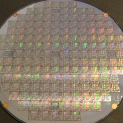
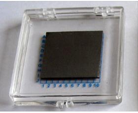
Single Crystal Germanium Wafer
PAM-XIAMEN offers 2”, 3”, 4” and 6” germanium wafer, which is short for Ge wafer grown by VGF / LEC. Lightly doped N and P type Germanium wafer can be also used for Hall effect experiment. At room temperature, crystalline germanium is brittle and has little plasticity. Germanium has semiconductor properties. High-purity germanium is doped with trivalent elements (such as indium, gallium, boron) to obtain P-type germanium semiconductors; and pentavalent elements (such as antimony, arsenic, and phosphorus) are doped to obtain N-type germanium semiconductors. Germanium has good semiconductor properties, such as high electron mobility and high hole mobility.
1. Properties of Germanium Wafer
1.1 General Properties of Germanium Wafer
| Generelt Egenskaber Struktur | Cubic, a = 5.6754 Å | ||
| Massefylde: 5,765 g / cm3 | |||
| Melting Point: 937.4 oC | |||
| Varmeledningsevne: 640 | |||
| Crystal Growth Teknologi | Czochralski | ||
| doping tilgængelig | / | Sb Doping | Doping I eller Ga |
| Ledende type | N | N | P |
| Specifik modstand, ohm.cm | >35 | <0,05 | 0,05-0,1 |
| EPD | < 5×10³/cm2 | < 5×10³/cm2 | < 5×10³/cm2 |
| < 5×10²/cm2 | < 5×10²/cm2 | < 5×10²/cm2 | |
1.2 Grades and Application of Germanium wafer
| Elektronisk Grade | Bruges til dioder og transistorer, |
| Infrarød eller opitical Grade | Bruges til IR optisk vindue eller diske, opitical komponenter |
| Cell Grade | Used for substrates of solar cell |
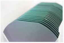
1.3 Standard Specs of Germanium Crystal and wafer
| Crystal Orientering | <111>,<100> and <110> ± 0.5o or custom orientation | |||
| Crystal boule som voksen | 1 "~ 6" diameter x 200 mm Længde | |||
| Standardblank som cut | 1 "x 0,5 mm | 2 "x0.6mm | 4 "x0.7mm | 5 "& 6" x0.8mm |
| Standard poleret wafer (en / to sider poleret) | 1 "x 0,30 mm | 2 "x0.5mm | 4 "x0.5mm | 5″&6″x0.6mm |
- Special size and orientation are available upon requested Wafers
2. Specification of Germanium Wafer
2.1 Specification of Germanium Wafer of 2”,3”,4”and 6”size
| Vare | Specifikationer | Bemærkninger |
| vækst Metode | VGF | — |
| varmeledning type | n-type, p type | |
| dopingmiddel | Gallium eller antimon | — |
| wafer i diameter | 2, 3,4 & 6 | inch |
| Crystal Orientering | (100), (111), (110) | — |
| Tykkelse | 200 ~ 550 | um |
| AF | EJ eller USA | — |
| Carrier Koncentration | anmodning ved kunderne | |
| Resistivity ved RT | (0,001 ~ 80) | Ohm.cm |
| Etch Pit Density | <5000 | / cm2 |
| Laser Mærkning | efter anmodning | — |
| Surface Finish | P / E eller P / P | — |
| Epi klar | Ja | — |
| Pakke | Enkelt wafer beholder eller kassette | — |
2.2 Germanium Wafer for Solar Cell
| 4 tommer Ge wafer Specification | for solceller | — |
| Doping | P | — |
| dopingmidler | Ge-Ga | — |
| Diameter | 100 ± 0,25 mm | — |
| Orientering | (100) 9 ° off mod <111> +/- 0,5 | |
| Off-orientering hældningsvinkel | N / A | — |
| Primær Flad Orientering | N / A | — |
| Primær Flad Længde | 32 ± 1 | mm |
| Sekundær Flad Orientering | N / A | — |
| Sekundær Flad Længde | N / A | mm |
| cc | (0,26-2,24) E18 | / cc |
| Resistivity | (0,74-2,81) E-2 | ohm.cm |
| Electron Mobility | 382-865 | cm2 / vs |
| EPD | <300 | / cm2 |
| Laser Mark | N / A | — |
| Tykkelse | 175 ± 10 | um |
| TTV | <15 | um |
| TIR | N / A | um |
| SLØJFE | <10 | um |
| Warp | <10 | um |
| Front ansigt | Poleret | — |
| Tilbage ansigt | Jord | — |
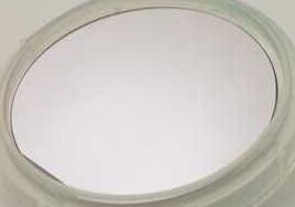
2.3 Ge Wafer (as an optical filter substrate for a longpass SWIR filter)
PAM180212-GE
| Vare | DSP Ge Wafer |
| Dia | 4” |
| Tykkelse | 1.50mm +/- 0.10mm |
| Orientering | N / A |
| Conductivity | N / A |
| Resistivity | N / A |
| Surface Process | Double-side polished; minimum 90mm dia. central clear aperture |
| Other Parameters | 60-40 scratch-dig or better |
| Less than 2 arc minutes parallelism | |
| Surfaces optically flat to within 1 fringe irregular per any 25mm dia. in the clear aperture |
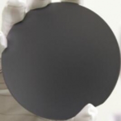
2.4 Germanium Used as Thin FIR Window (PAM211121-GE)
4″ Germanium wafer with low plasma frequency, 175µm+/-25um. (100), single side polished.
3. Germanium Wafer Process
With the advancement of science and technology, the processing technique of germanium wafer manufacturers is more and more mature. In the production of germanium wafers, germanium dioxide from the residue processing is further purified in chlorination and hydrolysis steps.
1) høj renhed germanium opnås under zone raffinering.
2) En germanium krystal er produceret via Czochralski-processen.
3) germanium wafer fremstilles via adskillige skæring, slibning, og ætsning trin.
4) Waferne rengøres og inspektion. I løbet af denne proces, de vafler er enkelt side poleret eller dobbelt side poleret efter sædvane krav, epi-klar wafer kommer.
5)The thin germanium wafers are packed in single wafer containers, under a nitrogen atmosphere.
4. Application of Germanium:
Germanium blank eller vindue anvendes i nattesyn og termografiske imaging-løsninger til kommerciel sikkerhed, brandslukning og industrielt udstyr overvågning. Også, at de anvendes som filtre til analytisk og måleudstyr, vinduer til måling remote temperatur samt spejle til lasere.
Thin Germanium substrates are used in III-V triple-junction solar cells and for power Concentrated PV (CPV) systems and as an optical filter substrate for a longpass SWIR filter application.
5. Test of Germanium Wafer:
The resistivity of the crystal germanium wafer was measured by Four Probe Resistance Tester, and the surface roughness of Germanium was measured by profilometer.
Remark:
The Chinese government has announced new limits on the exportation of Gallium materials (such as GaAs, GaN, Ga2O3, GaP, InGaAs, and GaSb) and Germanium materials used to make semiconductor chips on July 3, 2023. Exporting these materials is only allowed if we obtains a license from the Chinese Ministry of Commerce. Hope for your understanding and cooperation!

For more information, please contact us email at victorchan@powerwaywafer.com and powerwaymaterial@gmail.com.
P Type Thin Germanium Wafer | Solar Cell
Germanium Substrate for Optics and Epi-growth
Doped or Undoped Germanium (Ge) Crystal | Ge Single Crystal Growth
Single Crystal Germanium Wafer with Orientation (110) toward<111>
Test Method for Dislocation Density of Monocrystal Germanium
Du kan også gerne ...
-
Nanofabrikationsfotoresist
PAM-XIAMEN Tilbud fotoresist plade med fotoresist
-
GaN baserede LED Epitaksial Wafer
PAM-XIAMEN s GaN (galliumnitrid) -baseret LED epitaxial wafer er for ultrahøj lysstyrke blå og grønne lysdioder (LED) og laser dioder (LD) ansøgning.
-
Epitaksial Silicon Wafer
Silicon Epitaxial Wafer (Epi Wafer) er et lag af epitaksial silicium enkeltkrystal aflejret på en enkeltkrystal siliciumwafer (bemærk: det er tilgængeligt at dyrke et lag af polykrystallinsk siliciumlag oven på en højtdoteret enkeltkrystallinsk siliciumwafer, men det har brug for bufferlag (såsom oxid eller poly-Si) mellem bulk-Si-substratet og det øverste epitaksiale siliciumlag. Det kan også bruges til tyndfilmtransistor.
-
InSb wafer
PAM-XIAMEN offers Compound Semiconductor InSb wafer – Indium antimonide wafer which is grown by LEC(Liquid Encapsulated Czochralski) as epi-ready or mechanical grade with n type, p type or semi-insulating in different orientation(111) or (100). Indium antimonide doped with isoelectronic(such as N doping) can reduce the defect density during the indium antimonide thin films manufacturing process.
-
SiC Wafer Substrat
The company has a complete SiC(silicon carbide) wafer substrate production line integrating crystal growth, crystal processing, wafer processing, polishing, cleaning and testing. Nowadays we supply commercial 4H and 6H SiC wafers with semi insulation and conductivity in on-axis or off-axis, available size:5x5mm2,10x10mm2, 2”,3”,4”, 6” and 8″, breaking through key technologies such as defect suppression, seed crystal processing and rapid growth, promoting basic research and development related to silicon carbide epitaxy, devices, etc.
-
GaAs Epiwafer
PAM-XIAMEN fremstiller forskellige typer epi wafer III-V siliciumdoteret n-type halvledermaterialer baseret på Ga, Al, In, As og P dyrket af MBE eller MOCVD. Vi leverer tilpassede GaAs epiwafer-strukturer for at opfylde kundernes specifikationer, kontakt os venligst for mere information.
-
GaN Skabeloner
PAM-Xiamen Skabelon produkter består af krystallinske lag (galliumnitrid) GaN skabeloner, (aluminium nitrid) AlN skabelon, (aluminium galliumnitrid) AlGaN skabeloner og (indium gallium nitrid) InGaN skabeloner, som er deponeret på safir -
CdZnTe (CdZnTe) Wafer
Cadmium (CdZnTe eller CdZnTe) er en ny halvleder, som gør det muligt at konvertere stråling til elektron effektivt er den hovedsagelig anvendes i infrarødt tyndfilm-epitaxi substrat, X-ray detektorer og Gamma-ray CdZnTe-detektorer.