Ge (germanium) cristaux simples et Wafers
- La description
Description du produit
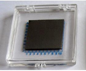
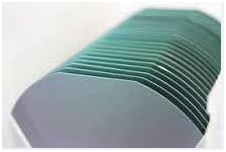
Single Crystal Germanium Wafer
PAM-XIAMEN offers 2”, 3”, 4” and 6” germanium wafer, which is short for Ge wafer grown by VGF / LEC. Lightly doped N and P type Germanium wafer can be also used for Hall effect experiment. At room temperature, crystalline germanium is brittle and has little plasticity. Germanium has semiconductor properties. High-purity germanium is doped with trivalent elements (such as indium, gallium, boron) to obtain P-type germanium semiconductors; and pentavalent elements (such as antimony, arsenic, and phosphorus) are doped to obtain N-type germanium semiconductors. Germanium has good semiconductor properties, such as high electron mobility and high hole mobility.
1. Properties of Germanium Wafer
1.1 General Properties of Germanium Wafer
| Structure Propriétés générales | Cubic, a = 5.6754 Å | ||
| Densité: 5,765 g / cm3 | |||
| Melting Point: 937.4 oC | |||
| La conductivité thermique: 640 | |||
| Crystal Technology Growth | Czochralski | ||
| dopage disponible | / | Sb dopage | Dopage ou Ga |
| type de Conductive | N | N | P |
| Résistivité, ohm.cm | >35 | <0,05 | De 0,05 à 0,1 |
| EPD | < 5×10³/cm2 | < 5×10³/cm2 | < 5×10³/cm2 |
| < 5×10²/cm2 | < 5×10²/cm2 | < 5×10²/cm2 | |
1.2 Grades and Application of Germanium wafer
| Niveau électronique | Utilisé pour des diodes et des transistors, |
| Niveau infrarouge ou opitical | Utilisé pour la fenêtre optique IR ou disques, composants opitical |
| Niveau cellulaire | Used for substrates of solar cell |
1.3 Standard Specs of Germanium Crystal and wafer
| cristal Orientation | <111>,<100> and <110> ± 0.5o or custom orientation | |||
| Cristal Grown Boulé | 1 diamètre "~ 6" x 200 mm Longueur | |||
| blanc standard coupe | 1 "x 0,5 mm | 2 "x0.6mm | 4 "x0.7mm | 5 "et 6" x0.8mm |
| plaquette polie standard (un / deux faces polies) | 1 "x 0,30 mm | 2 "x0.5mm | 4 "x0.5mm | 5″&6″x0.6mm |
- Special size and orientation are available upon requested Wafers
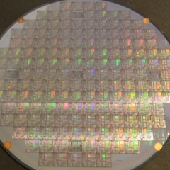
2. Specification of Germanium Wafer
2.1 Specification of Germanium Wafer of 2”,3”,4”and 6”size
| Article | Caractéristiques | Remarques |
| Procédé de croissance | VGF | — |
| Type de Conduction | n-type, p type | |
| dopant | Gallium ou Antimoine | — |
| wafer Diamter | 2, 3,4 et 6 | pouce |
| cristal Orientation | (100), (111), (110) | — |
| Épaisseur | 200 ~ 550 | um |
| DE | EJ ou US | — |
| Concentration porteuse | demande sur les clients | |
| Résistivité à la température ambiante | (0,001 ~ 80) | Ohm.cm |
| Etch Densité Pit | <5000 | / cm2 |
| Marquage laser | à la demande | — |
| Finition de surface | P / E ou P / P | — |
| Epi prêt | Oui | — |
| Paquet | récipient de plaquettes à l'unité ou de la cassette | — |
2.2 Germanium Wafer for Solar Cell
| plaquette 4 pouces Ge Spécification | pour les cellules solaires | — |
| Se doper | P | — |
| Les substances dopantes | Ge-Ga | — |
| Diamètre | 100 ± 0,25 mm | — |
| Orientation | (100) 9 ° au loin vers <111> +/- 0,5 | |
| angle d'inclinaison hors orientation | N / A | — |
| Orientation Plat principal | N / A | — |
| Plat Longueur primaire | 32 ± 1 | mm |
| Orientation Plat secondaire | N / A | — |
| Plat Longueur secondaire | N / A | mm |
| cc | (0,26 à 2,24) E18 | / cc |
| Résistivité | (0,74 à 2,81) E-2 | ohm.cm |
| Mobilité électronique | 382-865 | cm2 / vs |
| EPD | <300 | / cm2 |
| laser Mark | N / A | — |
| Épaisseur | 175 ± 10 | um |
| TTV | <15 | um |
| TIR | N / A | um |
| ARC | <10 | um |
| Chaîne | <10 | um |
| Face avant | Brillant | — |
| Face arrière | Sol | — |
2.3 Ge Wafer (as an optical filter substrate for a longpass SWIR filter)
PAM180212-GE
| Article | DSP Ge Wafer |
| Dia | 4” |
| Épaisseur | 1.50mm +/- 0.10mm |
| Orientation | N / A |
| Conductivity | N / A |
| Résistivité | N / A |
| Surface Process | Double-side polished; minimum 90mm dia. central clear aperture |
| Other Parameters | 60-40 scratch-dig or better |
| Less than 2 arc minutes parallelism | |
| Surfaces optically flat to within 1 fringe irregular per any 25mm dia. in the clear aperture |
2.4 Germanium Used as Thin FIR Window (PAM211121-GE)
4″ Germanium wafer with low plasma frequency, 175µm+/-25um. (100), single side polished.
3. Germanium Wafer Process
With the advancement of science and technology, the processing technique of germanium wafer manufacturers is more and more mature. In the production of germanium wafers, germanium dioxide from the residue processing is further purified in chlorination and hydrolysis steps.
1) le germanium de haute pureté est obtenu au cours du raffinage de la zone.
2) On réalise un cristal de germanium par le procédé de Czochralski.
3) La plaquette de germanium est fabriquée par plusieurs coupe, le meulage, et les étapes de gravure.
4) Les plaquettes sont nettoyées et l'inspection. Au cours de ce processus, les plaquettes sont polies côté ou double côté lustrés selon l'exigence personnalisée, plaquette epi prêt vient.
5)The thin germanium wafers are packed in single wafer containers, under a nitrogen atmosphere.
4. Application of Germanium:
Germanium blanc ou fenêtre sont utilisés dans la vision nocturne et des solutions d'imagerie thermographiques pour la sécurité commerciale, lutte contre l'incendie et de l'équipement de surveillance industrielle. Ils sont également utilisés en tant que filtres pour appareils d'analyse et de mesure, des fenêtres de mesure de température à distance et un miroir pour laser.
Thin Germanium substrates are used in III-V triple-junction solar cells and for power Concentrated PV (CPV) systems and as an optical filter substrate for a longpass SWIR filter application.
5. Test of Germanium Wafer:
The resistivity of the crystal germanium wafer was measured by Four Probe Resistance Tester, and the surface roughness of Germanium was measured by profilometer.
Remark:
The Chinese government has announced new limits on the exportation of Gallium materials (such as GaAs, GaN, Ga2O3, GaP, InGaAs, and GaSb) and Germanium materials used to make semiconductor chips on July 3, 2023. Exporting these materials is only allowed if we obtains a license from the Chinese Ministry of Commerce. Hope for your understanding and cooperation!

For more information, please contact us email at victorchan@powerwaywafer.com and powerwaymaterial@gmail.com.
P Type Thin Germanium Wafer | Solar Cell
Germanium Substrate for Optics and Epi-growth
Doped or Undoped Germanium (Ge) Crystal | Ge Single Crystal Growth
Single Crystal Germanium Wafer with Orientation (110) toward<111>
Test Method for Dislocation Density of Monocrystal Germanium
Vous aimerez aussi ...
-
CdZnTe (CZT) Wafer
Cadmium Zinc Telluride (CdZnTe ou CZT) est un nouveau semi-conducteur, ce qui permet de convertir un rayonnement à électrons efficace, il est principalement utilisé dans le substrat d'épitaxie en couche mince infrarouge, des détecteurs à rayons X et les détecteurs de rayons gamma CdZnTe. -
Substrat de tranche de SiC
La société dispose d'une ligne complète de production de substrats de plaquettes SiC (carbure de silicium) intégrant la croissance cristalline, le traitement des cristaux, le traitement des plaquettes, le polissage, le nettoyage et les tests. Aujourd'hui, nous fournissons des plaquettes SiC commerciales 4H et 6H avec semi-isolation et conductivité sur axe ou hors axe, tailles disponibles : 5x5 mm2, 10x10 mm2, 2", 3", 4", 6" et 8", perçant des technologies clés telles que comme la suppression des défauts, le traitement des germes de cristal et la croissance rapide, favorisant la recherche et le développement fondamentaux liés à l'épitaxie du carbure de silicium, aux dispositifs, etc.
-
Photoréserve de nanofabrication
PAM-XIAMEN Offres plaque de résine photosensible avec résine photosensible
-
Modèles GaN
PAM-Xiamen les Modèles de produits constitués de couches cristallines de (nitrure de gallium) modèles GaN, (nitrure d'aluminium) modèle de AlN, (nitrure de gallium aluminium) modèles de AlGaN et (nitrure de gallium indium) modèles de InGaN, qui sont déposés sur saphir -
GaN à base de LED épitaxiales Wafer
GaN de PAM-XIAMEN (nitrure de gallium) à base de plaquette épitaxiale de LED est de très haute luminosité de lumière bleue et verte diodes électroluminescentes (LED) et des diodes laser d'application (LD).
-
plaquette InSb
PAM-XIAMEN propose une plaquette InSb à semi-conducteur composé – une plaquette d'antimonide d'indium qui est cultivée par LEC (Liquid Encapsulated Czochralski) en tant que qualité épi-prête ou mécanique avec type n, type p ou semi-isolant dans différentes orientations (111) ou (100). L'antimonide d'indium dopé avec de l'isoélectronique (tel que le dopage N) peut réduire la densité des défauts pendant le processus de fabrication de films minces d'antimonure d'indium.
-
Silicon Wafer épitaxial
Silicon Epitaxial Wafer(Epi Wafer) is a layer of epitaxial silicon single crystal deposited onto a single crystal silicon wafer(note: it is available to grow a layer of poly crystalline Silicon layer on top of a highly doped Singly crystalline silicon wafer, but it needs buffer layer (such as oxide or poly-Si) in between the bulk Si substrate and the top epitaxial silicon layer. It also can be used for thin film transistor.
-
GaAs tranches épitaxiées
PAM-XIAMEN is manufacturing various types of epi wafer III-V silicon doped n-type semiconductor materials based on Ga, Al, In, As and P grown by MBE or MOCVD. We supply custom GaAs epiwafer structures to meet customer specifications, please contact us for more information.