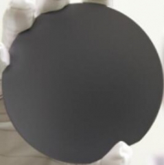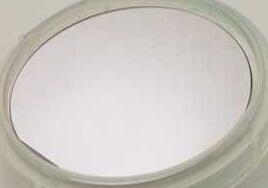

GaN-baseret LED Epitaxial Wafer
PAM-XIAMEN s GaN (galliumnitrid) -baseret LED epitaxial wafer er for ultrahøj lysstyrke blå og grønne lysdioder (LED) og laser dioder (LD) ansøgning.
- Beskrivelse
Beskrivelse
The LED epitaxial wafer is a substrate heated to an appropriate temperature. The LED wafer material is the cornerstone of the technology development for the semiconductor lighting industry. Different substrate materials require different LED epitaxial wafer growth technology, chip processing technology and device packaging technology. The substrate for LED epi wafer determines the development route of semiconductor lighting technology. To achieve luminous efficiency, epitaxial wafer suppliers pay more attention to GaN based LED epitaxial wafer, since the epitaxial wafer price is in low cost, and the epi wafer defect density is small. LED epi wafer advantage on GaN substrate is the realization of high efficiency, large area, single lamp and high power, which make the process technology simplify and improve the large yield rate. The development prospects of the LED epi wafer market are optimistic.
1. LED Wafer List
|
LED Epitaxial Wafer |
||||||||
| Vare | Size | Orientering | Emission | Wavelength | Thickness | Substrate | Surface | Usable area |
| PAM-50-LED-BLUE-F | 50mm | 0°±0.5° | blue light | 445-475nm | 425um+/-25um | Sapphire | P/L | >90% |
| PAM-50-LED-BLUE-PSS | 50mm | 0°±0.5° | blue light | 445-475nm | 425um+/-25um | Sapphire | P/L | >90% |
| PAM-100-LED-BLUE-F | 100mm | 0°±0.5° | blue light | 445-475nm | / | Sapphire | P/L | >90% |
| PAM-100-LED-BLUE-PSS | 100mm | 0°±0.5° | blue light | 445-475nm | / | Sapphire | P/L | >90% |
| PAM-150-LED-BLUE | 150mm | 0°±0.5° | blue light | 445-475nm | / | Sapphire | P/L | >90% |
| PAM-100-LED-BLUE-SIL | 50mm | 0°±0.5° | blue light | 445-475nm | / | Silicon | P/L | >90% |
| PAM-100-LED-BLUE-SIL | 100mm | 0°±0.5° | blue light | 445-475nm | / | Silicon | P/L | >90% |
| PAM-150-LED-BLUE-SIL | 150mm | 0°±0.5° | blue light | 445-475nm | / | Silicon | P/L | >90% |
| PAM-200-LED-BLUE-SIL | 200mm | 0°±0.5° | blue light | 445-475nm | / | Silicon | P/L | >90% |
| PAM-50-LED-GREEN-F | 50mm | 0°±0.5° | green light | 510-530nm | 425um+/-25um | Sapphire | P/L | >90% |
| PAM-50-LED-GREEN-PSS | 50mm | 0°±0.5° | green light | 510-530nm | 425um+/-25um | Sapphire | P/L | >90% |
| PAM-100-LED-GREEN-F | 100mm | 0°±0.5° | green light | 510-530nm | / | Sapphire | P/L | >90% |
| PAM-100-LED-GREEN-PSS | 100mm | 0°±0.5° | green light | 510-530nm | / | Sapphire | P/L | >90% |
| PAM-150-LED-GREEN | 150mm | 0°±0.5° | green light | 510-530nm | / | Sapphire | P/L | >90% |
| PAM-100-LED-RED-GAAS-620 | 100mm | 15°±0.5° | red light | 610-630nm | / | GaAs | P/L | >90% |
| PAM210527-LED-660 | 100mm | 15°±0.5° | red light | 660nm | / | GaAs | P/L | >90% |
| PAM-210414-850nm-LED | 100mm | 15°±0.5° | IR | 850nm | / | GaAs | P/L | >90% |
| PAMP21138-940LED | 100mm | 15°±0.5° | IR | 940nm | / | GaAs | P/L | >90% |
| PAM-50-LED-UV-365-PSS | 50mm | 0°±0.5° | UVA | 365 nm | 425um+/-25um | Sapphire | ||
| PAM-50-LED-UV-405-PSS | 50mm | 0°±0.5° | UVA | 405 nm | 425um+/-25um | Sapphire | ||
| PAM-50-LED-UVC-275-PSS | 50mm | 0°±0.5° | UVC | 275nm | 425um+/-25um | Sapphire | ||
| PAM-50-LD-UV-405-SIL | 50mm | 0°±0.5° | UV | 405nm | / | Silicon | P/L | >90% |
| PAM-50-LD-BLUE-450-SIL | 50mm | 0°±0.5° | blue light | 450nm | / | Silicon | P/L | >90% |
As a LED epitaxial wafer manufacturer, PAM-XIAMEN can offer activated and unactivated GaN Epi LED wafer for LED and laser diodes (LD) application,such as For micro LED or ultra thin wafer or UV LED researches or LED manufacturers. LED epitaxial wafer on GaN is grown by MOCVD with PSS or flat sapphire for LCD back light, mobile, electronic or UV(ultraviolet), with blue or green or red emission, including InGaN/GaN active area and AlGaN layers with GaN well/AlGaN barrier for different chip sizes.
2. InGaN/GAN(gallium nitride) based LED Epitaxial Wafer
GaN på Al2O3-2 ”epi wafer Specification (LED Epitaxial wafer)
| Hvid : 445 ~ 460 nm |
| Blå : 465 ~ 475 nm |
| Grøn : 510 ~ 530 nm |
1. Vækstteknik - MOCVD
2. Skivediameter: 50,8 mm
3. Underlagsmateriale til wafer: mønstret safirunderlag (Al2O3) eller flad safir
4. Skivemønsterstørrelse: 3X2X1,5μm
3. Wafer structure:
| Strukturlag | Tykkelse (um) |
| p-GaN | 0.2 |
| p-AlGaN | 0.03 |
| InGaN / GaN (aktivt område) | 0.2 |
| n-gan | 2.5 |
| u-GaN | 3.5 |
| Al2O3 (underlag) | 430 |
4. Wafer parameters to make chips:
| em | Farve | Chip Størrelse | Egenskaber | Udseende | |
| PAM1023A01 | Blå | 10m x 23mil |  |
Belysning | |
| Vf = 2,8 ~ 3,4 V | LCD baggrundsbelysning | ||||
| Po = 18 ~ 25 mW | Mobil apparater | ||||
| Wd = 450 ~ 460 nm | Forbruger elektronisk | ||||
| PAM454501 | Blå | 45mil x 45mil | Vf = 2,8 ~ 3,4 V |  |
Generel belysning |
| Po = 250 ~ 300 mW | LCD baggrundsbelysning | ||||
| Wd = 450 ~ 460 nm | Udendørs display |
5. Application of LED epitaixal wafer:
*If you need to know more detail information of Blue LED Epitaxial Wafer, please contact with our sales departments
Belysning
LCD baggrundslys
Mobil apparater
Forbruger elektronisk
6. Specification of LED Epi Wafer as an example:
Spec PAM190730-LED
– size : 4 inch
– WD : 455 ± 10nm
– brightness : > 90mcd
– VF : < 3.3V
– n-GaN Thickness : <4.1㎛
– u-GaN thickness : <2.2㎛
– substrate : patterned sapphire substrate (PSS)
7.GaAs(Gallium arsenide)based LED Wafer Material:
Med hensyn til GaAs LED-skive, dyrkes de af MOCVD, se nedenfor bølgelængde for GaAs LED-skive:
Rød: 585nm, 615nm, 620 ~ 630nm
Yellow:587 ~ 592nm
Yellow/Green: 568 ~ 573nm
8. Definition of LED Epitaxial Wafer:
What we offer is bare LED epi wafer or not processed wafer without lithography processes, n- and metals contacts, etc. And you can fabricate the LED chip using your fabrication equipment for different application such as nano optoelectronics research.
Remark:
The Chinese government has announced new limits on the exportation of Gallium materials (such as GaAs, GaN, Ga2O3, GaP, InGaAs, and GaSb) and Germanium materials used to make semiconductor chips. Starting from August 1, 2023, exporting these materials is only allowed if we obtains a license from the Chinese Ministry of Commerce. Hope for your understanding and cooperation!
For disse detaljer GaAs LED wafer specs, kan du besøge:GaAs Epi Wafer til LED
For UV-LED-pladespecifikationer, skal du besøge:UV LED Epi Wafer
For LED-skive på siliciumspecifikationer skal du besøge:LED Wafer på silicium
For Blue GaN LD Wafer-specifikationer skal du besøge: Blue GaN LD Wafer
For Violet GaN LD Wafer, please visit: 405nm GaN Laser Diode Wafer
850nm and 940nm infrared LED wafer
850-880nm and 890-910nm Red Infrared AlGaAs /GaAs LED Epi-Wafer
GaN Wafers to Fabricate LED Devices
GaN LED Structure Epitaxy on Flat or PSS Sapphire Substrate
GaN Epitaxial Growth on Sapphire for LED
Formation of V-Shaped Pits in Nitride Films Grown by Metalorganic Chemical Vapor Deposition
Si-based GaN PIN Photodetector Structure
For more foundry services, please visit: GaN Foundry Services for LED Fabrication
Du kan også gerne ...
-
GaAs Epiwafer
PAM-XIAMEN fremstiller forskellige typer epi wafer III-V siliciumdoteret n-type halvledermaterialer baseret på Ga, Al, In, As og P dyrket af MBE eller MOCVD. Vi leverer tilpassede GaAs epiwafer-strukturer for at opfylde kundernes specifikationer, kontakt os venligst for mere information.
-
SiC Wafer Substrat
The company has a complete SiC(silicon carbide) wafer substrate production line integrating crystal growth, crystal processing, wafer processing, polishing, cleaning and testing. Nowadays we supply commercial 4H and 6H SiC wafers with semi insulation and conductivity in on-axis or off-axis, available size:5x5mm2,10x10mm2, 2”,3”,4”, 6” and 8″, breaking through key technologies such as defect suppression, seed crystal processing and rapid growth, promoting basic research and development related to silicon carbide epitaxy, devices, etc.
-
GaN Skabeloner
PAM-Xiamen Skabelon produkter består af krystallinske lag (galliumnitrid) GaN skabeloner, (aluminium nitrid) AlN skabelon, (aluminium galliumnitrid) AlGaN skabeloner og (indium gallium nitrid) InGaN skabeloner, som er deponeret på safir -
Fritstående GaN-substrat
PAM-XIAMEN har etableret den fremstillingsteknologi til fritstående (galliumnitrid) GaN substratwafer, der er til UHB-LED og LD. Vokset med hydrid dampfase epitaxy (HVPE) teknologi, Vores GaN substrat har lav defekt tæthed.
-
InSb wafer
PAM-XIAMEN offers Compound Semiconductor InSb wafer – Indium antimonide wafer which is grown by LEC(Liquid Encapsulated Czochralski) as epi-ready or mechanical grade with n type, p type or semi-insulating in different orientation(111) or (100). Indium antimonide doped with isoelectronic(such as N doping) can reduce the defect density during the indium antimonide thin films manufacturing process.
-
GaN HEMT Epitaksial Wafer
Gallium Nitride (GaN) HEMTs (High Electron Mobility Transistors) are the next generation of RF power transistor technology. Thanks to GaN technology, PAM-XIAMEN now offer AlGaN/GaN HEMT Epi Wafer on sapphire or Silicon, and AlGaN/GaN on sapphire template.
-
Ge (Germanium) enkelte krystaller og Wafers
PAM-XIAMEN tilbyder 2”, 3”, 4” og 6” germanium wafer, som er en forkortelse for Ge wafer dyrket af VGF / LEC. Let dopet Germanium wafer af P og N type kan også bruges til Hall effekt eksperiment. Ved stuetemperatur er krystallinsk germanium skørt og har ringe plasticitet. Germanium har halvlederegenskaber. Germanium med høj renhed er dopet med trivalente grundstoffer (såsom indium, gallium, bor) for at opnå P-type germanium-halvledere; og pentavalente grundstoffer (såsom antimon, arsen og phosphor) er dopet for at opnå N-type germanium-halvledere. Germanium har gode halvlederegenskaber, såsom høj elektronmobilitet og høj hulmobilitet. -
Cz Mono-krystallinsk silicium
PAM-XIAMEN, en monokrystallinsk bulk silicium producent, kan tilbyde <100>, <110> og <111> monokrystallinske silicium wafers med N&P doteringsmiddel i 76,2~200 mm, som dyrkes ved CZ metode. Czochralski-metoden er en krystalvækstmetode, kaldet CZ-metoden. Den er integreret i et varmesystem med lige rør, opvarmet af grafitmodstand, smelter polysilicium indeholdt i en højrent kvartsdigel og indsætter derefter frøkrystallen i overfladen af smelten til svejsning. Derefter sænkes den roterende frøkrystal og smeltes. Kroppen infiltreres og røres, hæves gradvist og afsluttes eller trækkes gennem trinene med halsudskæring, halsudskæring, skulderring, kontrol med samme diameter og efterbehandling.