PAM-شيامن offers PSS patterned sapphire substrate for high brightness GaN based LED EPI growing application. The patterned sapphire substrate wafer هو زراعة قناع حفر جاف على طبقة من الياقوت الأزرق. تم نقش القناع بواسطة عملية طباعة حجرية ضوئية قياسية. ثم يتم حفر الياقوت بواسطة تقنية النقش ICP ، وفي غضون ذلك ، تتم إزالة القناع. بعد ذلك ، تزرع مادة GaN على الياقوت ، بحيث تصبح epitaxy العمودي لمادة GaN هي النتوء الأفقي. تفاصيل الركيزة الزفير المزخرفة أدناه:
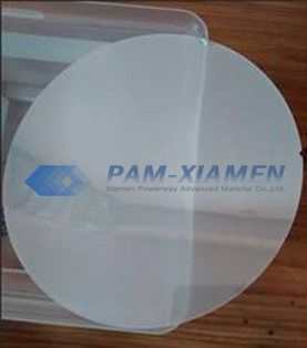
الركيزة PSS الياقوت
1.Sانتزاعق من الركيزة الياقوت منقوشة
| المعلمات | مواصفات | وحدة |
| مادة | أحادي البلورية عالية النقاء | |
| قطر | 50.8 ± 0.1 | ㎜ |
| سماكة | 430 ± 10 | ㎛ |
| تباين السماكة الكلي | ≤10 | ㎛ |
| الطول الأساسي المسطح | 16.0 ± 1.0 | ㎜ |
| الاتجاه الأساسي المسطح | طائرة ± 0.2 | |
| جودة السطح الأمامي | Epitaxial جاهز | |
| خشونة السطح الخلفي | 1.0 ± 0.1 | ㎛ |
| اتجاه السطح أ | 0˚off ± 0.1 | |
| اتجاه السطح م | 0.2˚off ± 0.10 | |
| اتجاه السطح R | R9 | |
| ينحني | -10 ~ 0 | ㎛ |
| اعوجاج | ≤15 | ㎛ |
| عرض النمط | 2.7 ± 0.15 | ㎛ |
| ارتفاع النمط | 1.7 ± 0.15 | ㎛ |
| نمط الملعب | 3.0 ± 0.05 | ㎛ |
2.لماذا تختار ركيزة منقوشة من الياقوت لمصباح LED؟
On the one hand, the cone-shaped patterned sapphire substrate wafer can effectively reduce the dislocation density of the GaN epitaxial material(the patterned sapphire substrate dislocation is low), thereby reducing the non-radiative recombination of the active area, reducing the reverse leakage current, and improving the life of the LED. On the other hand, the light emitted from the active region is scattered multiple times by the interface of GaN and sapphire substrate, and the exit angle of total reflection light is changed, increasing the probability that the light of the flip-chip LED emerges from the sapphire substrate, thereby improving the extraction efficiency of the light.
باختصار ، تم تحسين سطوع الضوء المنبعث من LED المزروع على ركيزة الياقوت المزخرفة بتقنية النانو بشكل كبير مقارنة بمصباح LED التقليدي. يتم تقليل تيار التسرب العكسي ، مما يطيل من عمر LED.
A patterned sapphire substrate belongs to the semiconductor industry. As a high-brightness epitaxial material, it is the source material of the LED lighting industry. Meanwhile, using PSS Al2O3 wafer to grow epitaxial wafers is the most effective way to improve the brightness of the chip. It is also the best choice for the high-power and high-brightness epitaxial wafers.

لمزيد من المعلومات ، يرجى الاتصال بنا على البريد الإلكتروني على victorchan@powerwaywafer.com و powerwaymaterial@gmail.com.