The structures of InxGa1-xAsyP1-y (indium gallium arsenide phosphide) quantum well epitaxially grown on InP substrate can be purchased or customized from PAM-XIAMEN. By adjusting the composition of x and y, the coverage wavelength range is from 870nm (GaAs) to 3.5um (InAs), which includes the optical [...]
2021-10-25méta-auteur
PAM XIAMEN offers 3″ Silicon Wafer.
Diameter
Type
Dopant
Growth
method
Orientation
Resistivity
Thickness
Surface
Grade
76.2
SI.
Undoped
VGF
-100
>1E7
600-650
P/E
PRIME
76.2
SI.
Undoped
VGF
-100
>1E7
610-660
P/P
EPI
76.2
N
Si
VGF
-100
600-650
P/E
PRIME
76.2
P
Zn
VGF
-100
600-650
P/E
PRIME
76.2
Undoped
CZ
-100
>30
300-350
P/P
EPI
76.2
Undoped
CZ
-100
>30
350-400
P/E
EPI
76.2
N
Sb
CZ
(100)-6
.01-.04
100-200
P/E
TEST
76.2
N
Sb
CZ
-100
.005-.02
300-350
P/P
EPI
76.2
N
Sb
CZ
-100
.005-.02
350-400
P/E
EPI
76.2
P
Ga
CZ
-100
.01-.04
300-350
P/P
EPI
76.2
P
Ga
CZ
-100
.01-.04
350-400
P/E
EPI
76.2
N
Si
VGF
-100
600-650
P/E
PRIME
76.2
P
Zn
VGF
-100
600-650
P/E
PRIME
76.2
Si
Fe
VGF
-100
5000000
600-650
P/E
PRIME
76.2
Single Wafer Shipper
ePak
Lid/Base/Spring
Holds1Wafer
Clean Room
76.2
Shipping Cassette
ePak
Holds25Wafers
Clean Room
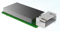
In addition, we can offer substrate used as Alpha Spectrometer Consumables:
Silicon substrate (PAM210610 – SI)
Main technical characteristics:
Material: silicon (can be replaced with quartz).
Diameter – (74.0 ± 0.5) mm.
Thickness – (0.5 ± 0.05) mm.
Grinding [...]
2019-03-04méta-auteur
With the sudden outbreak of COVID-19, some vertical categories that are not usually paid attention to quickly became popular. Materials related to epidemic prevention and control, such as masks, goggles, and disinfectant, have become popular. Among them, UVC (Ultra Violet C radiation) LED with [...]
2022-05-30méta-auteur
We are an expert of semiconductor wafers in semiconductor industry, and we offer technology support and wafers selling for thousands of univerisities and industrial customers by our decades experience, including Cornell University, Stanford Univeristy,Peking University, Shandong Univerity, university of south carolina,Caltech Faraon lab (USA),University of California, Irvine (USA),Singapore MIT Alliance for Research and Technology Centre (SMART),West Virginia University,Purdue Univerity, University of California, Los Angeles,King Abdullah University of Science & Technology,Massachusetts Institute of Technology,University of Houston,University of Wisconsin,University of Science and Technology of China etc.
And now we show one article example as follows, who bought our wafers or service:
Article title:GaN LEDs fabricated using SF6 plasma RIE
Published by:
Wasif Khan ; Xiaopeng Bi ; Bin Fan ; Wen Li
Department of Electrical and [...]
2019-12-02méta-auteur
Group III nitride materials are a kind of direct band gap materials, which have the advantages of wide band gap, strong chemical stability, high breakdown electric field and high thermal conductivity. They have broad application prospects in the fields of efficient light-emitting devices and [...]
2022-11-25méta-auteur
PAM-XIAMEN can offer 4” GaAs HEMT epi wafer with 2D electron gas (2DEG) and very high electron mobility of 5-7E5 cm2/V.s, please see below typical wafers of gallium arsenide with HEMT structure:
1. GaAs HEMT Epitaxial Wafer Structures
Structure 1: 4″ AlGaAs / GaAs HEMT epi wafer (PAM200416-HEMT):
HEMT [...]