Etching is a technique used for micromachining to chemically remove layers from the surface of a wafer during manufacturing. Etching techniques can be divided into wet etching and dry etching. PAM-XIAMEN can provide silicon etching wafer for your applications.
1. Wet Chemical Etching
The mechanism of wet chemical etching mainly includes three stages: the reactants diffuse to the surface of the reactants, the chemical reaction proceeds on the surface, and then the reaction products are removed from the surface by diffusion. The schematic diagram of wet chemical etching is shown as below:
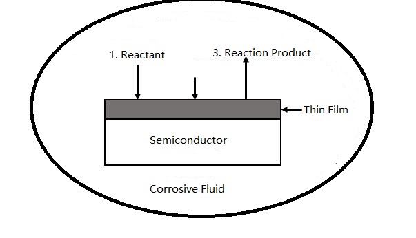
The stirring and temperature of the etching solution will affect the etching rate. In the integrated circuit process, most of the wet chemical etching is to immerse the silicon wafer in a chemical solvent or spray the etching solvent on the silicon wafer. For immersion etching, the silicon wafer is put into a chemical solvent, and stirring is required to ensure that the etching process is carried out at a consistent or constant rate; spray etching greatly increases by continuously supplying new etchants to the surface of the silicon wafer. For etching rate and consistency, spraying is better than immersion.
Wet chemical etching is more suitable for surface etching of polysilicon, oxides, nitrides, metals and III-V compounds.
2. Dry Etching
The biggest disadvantage of wet chemical etching in pattern transfer is that there will be lateral undercutting under the mask, resulting in a decrease in the resolution of the pattern after etching. In order to achieve the high-precision photoresist resist pattern transfer required by the process of larger-scale integrated circuits, dry etching has been rapidly developed.
Dry etching methods include plasma etching, reactive ion etching, sputter etching, magnetically enhanced reactive ion etching, reactive ion beam etching, high-density plasma etching, and etc.
Let’s briefly talk about plasma etching.
A plasma is a fully or partially ionized gas ion consisting of equal numbers of positive and negative charges and varying numbers of unionized molecules. Plasma is created when a sufficiently large electric field is applied to a gas to break down and ionize it. The plasma is triggered by free electrons, which can be emitted by negatively biased electrodes or generated by other methods. Free electrons gain kinetic energy from the electric field and lose energy by colliding with gas molecules during their movement through the gas. The energy transferred in the collision ionizes the gas molecules, creating free electrons. These free electrons in turn gain kinetic energy from the electric field, and the above process continues. Therefore, when the applied voltage is greater than the breakdown voltage, continuous plasma can be formed in the entire reaction chamber. The plasma used for dry etching has a relatively low electron concentration, and plasma-assisted dry etching is a low-temperature process.
The schematic diagram of several basic steps of plasma dry etching is as follows:
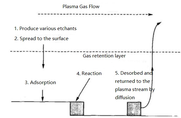
Plasma etching technology is based on plasma generated in a gas at low pressure. The two basic methods commonly used are physical methods and chemical methods. The former includes sputter etching and the latter includes pure chemical etching.
Dry etching is synonymous with plasma-assisted etching and is used for high-precision pattern transfer.

Per ulteriori informazioni potete contattarci via e-mail all'indirizzovictorchan@powerwaywafer.com e powerwaymaterial@gmail.com.