PAM-XIAMEN offers PSS patterned sapphire substrate for high brightness GaN based LED EPI growing application. The patterned sapphire substrate wafer é fazer crescer uma máscara de corrosão seca no substrato de safira. A máscara é gravada por um processo de fotolitografia padrão. Em seguida, a safira é gravada pela tecnologia de gravação ICP e, enquanto isso, a máscara é removida. Depois disso, o material GaN é cultivado na safira, de modo que a epitaxia vertical do material GaN se torna a epitaxia horizontal. Os detalhes do substrato de safira padronizado estão abaixo:
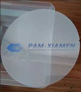
Substrato de safira PSS
1.Specificaçãos de Substrato de safira padronizado
| Parâmetros | Especificação | Unidade |
| Material | Al2O3 monocristalino de alta pureza | |
| Diâmetro | 50,8 ± 0,1 | ㎜ |
| Espessura | 430 ± 10 | ㎛ |
| Variação de espessura total | ≤10 | ㎛ |
| Comprimento plano primário | 16,0 ± 1,0 | ㎜ |
| Orientação plana primária | Um plano ± 0,2 | |
| Qualidade da superfície frontal | Epitaxial pronto | |
| Rugosidade da superfície posterior | 1,0 ± 0,1 | ㎛ |
| Orientação da superfície A | 0˚ desligado ± 0,1 | |
| Orientação da superfície M | 0,2˚ desligado ± 0,10 | |
| Orientação da superfície R | R9 | |
| ARCO | -10 ~ 0 | ㎛ |
| URDIDURA | ≤15 | ㎛ |
| Largura do Padrão | 2,7 ± 0,15 | ㎛ |
| Altura Padrão | 1,7 ± 0,15 | ㎛ |
| Pitch do padrão | 3,0 ± 0,05 | ㎛ |
2.Por que escolher substrato de safira com padrão para LED?
On the one hand, the cone-shaped patterned sapphire substrate wafer can effectively reduce the dislocation density of the GaN epitaxial material(the patterned sapphire substrate dislocation is low), thereby reducing the non-radiative recombination of the active area, reducing the reverse leakage current, and improving the life of the LED. On the other hand, the light emitted from the active region is scattered multiple times by the interface of GaN and sapphire substrate, and the exit angle of total reflection light is changed, increasing the probability that the light of the flip-chip LED emerges from the sapphire substrate, thereby improving the extraction efficiency of the light.
Em resumo, o brilho da luz emitida pelo LED que cresce no substrato de safira com padrão nano é muito melhorado do que o do LED tradicional. A corrente de fuga reversa é reduzida, estendendo a vida útil do LED.
A patterned sapphire substrate belongs to the semiconductor industry. As a high-brightness epitaxial material, it is the source material of the LED lighting industry. Meanwhile, using PSS Al2O3 wafer to grow epitaxial wafers is the most effective way to improve the brightness of the chip. It is also the best choice for the high-power and high-brightness epitaxial wafers.

Para obter mais informações, entre em contato conosco pelo e-mail victorchan@powerwaywafer.com and powerwaymaterial@gmail.com.