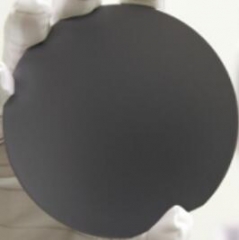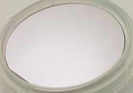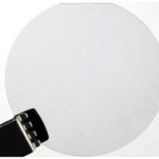
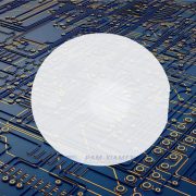

Wafer epitassiale LED basato su GaN
Il wafer epitassiale LED a base di GaN (nitruro di gallio) di PAM-XIAMEN è per applicazioni con diodi a emissione di luce blu e verde ad altissima luminosità (LED) e diodi laser (LD).
- Descrizione
Descrizione del prodotto
The LED epitaxial wafer is a substrate heated to an appropriate temperature. The LED wafer material is the cornerstone of the technology development for the semiconductor lighting industry. Different substrate materials require different LED epitaxial wafer growth technology, chip processing technology and device packaging technology. The substrate for LED epi wafer determines the development route of semiconductor lighting technology. To achieve luminous efficiency, epitaxial wafer suppliers pay more attention to GaN based LED epitaxial wafer, since the epitaxial wafer price is in low cost, and the epi wafer defect density is small. LED epi wafer advantage on GaN substrate is the realization of high efficiency, large area, single lamp and high power, which make the process technology simplify and improve the large yield rate. The development prospects of the LED epi wafer market are optimistic.
1. LED Wafer List
|
LED Epitaxial Wafer |
||||||||
| Voce | Size | Orientation | Emission | Wavelength | Thickness | Substrate | Surface | Usable area |
| PAM-50-LED-BLUE-F | 50mm | 0°±0.5° | blue light | 445-475nm | 425um+/-25um | Sapphire | P/L | >90% |
| PAM-50-LED-BLUE-PSS | 50mm | 0°±0.5° | blue light | 445-475nm | 425um+/-25um | Sapphire | P/L | >90% |
| PAM-100-LED-BLUE-F | 100mm | 0°±0.5° | blue light | 445-475nm | / | Sapphire | P/L | >90% |
| PAM-100-LED-BLUE-PSS | 100mm | 0°±0.5° | blue light | 445-475nm | / | Sapphire | P/L | >90% |
| PAM-150-LED-BLUE | 150mm | 0°±0.5° | blue light | 445-475nm | / | Sapphire | P/L | >90% |
| PAM-100-LED-BLUE-SIL | 50mm | 0°±0.5° | blue light | 445-475nm | / | Silicon | P/L | >90% |
| PAM-100-LED-BLUE-SIL | 100mm | 0°±0.5° | blue light | 445-475nm | / | Silicon | P/L | >90% |
| PAM-150-LED-BLUE-SIL | 150mm | 0°±0.5° | blue light | 445-475nm | / | Silicon | P/L | >90% |
| PAM-200-LED-BLUE-SIL | 200mm | 0°±0.5° | blue light | 445-475nm | / | Silicon | P/L | >90% |
| PAM-50-LED-GREEN-F | 50mm | 0°±0.5° | green light | 510-530nm | 425um+/-25um | Sapphire | P/L | >90% |
| PAM-50-LED-GREEN-PSS | 50mm | 0°±0.5° | green light | 510-530nm | 425um+/-25um | Sapphire | P/L | >90% |
| PAM-100-LED-GREEN-F | 100mm | 0°±0.5° | green light | 510-530nm | / | Sapphire | P/L | >90% |
| PAM-100-LED-GREEN-PSS | 100mm | 0°±0.5° | green light | 510-530nm | / | Sapphire | P/L | >90% |
| PAM-150-LED-GREEN | 150mm | 0°±0.5° | green light | 510-530nm | / | Sapphire | P/L | >90% |
| PAM-100-LED-RED-GAAS-620 | 100mm | 15°±0.5° | red light | 610-630nm | / | GaAs | P/L | >90% |
| PAM210527-LED-660 | 100mm | 15°±0.5° | red light | 660nm | / | GaAs | P/L | >90% |
| PAM-210414-850nm-LED | 100mm | 15°±0.5° | IR | 850nm | / | GaAs | P/L | >90% |
| PAMP21138-940LED | 100mm | 15°±0.5° | IR | 940nm | / | GaAs | P/L | >90% |
| PAM-50-LED-UV-365-PSS | 50mm | 0°±0.5° | UVA | 365 nm | 425um+/-25um | Sapphire | ||
| PAM-50-LED-UV-405-PSS | 50mm | 0°±0.5° | UVA | 405 nm | 425um+/-25um | Sapphire | ||
| PAM-50-LED-UVC-275-PSS | 50mm | 0°±0.5° | UVC | 275nm | 425um+/-25um | Sapphire | ||
| PAM-50-LD-UV-405-SIL | 50mm | 0°±0.5° | UV | 405nm | / | Silicon | P/L | >90% |
| PAM-50-LD-BLUE-450-SIL | 50mm | 0°±0.5° | blue light | 450nm | / | Silicon | P/L | >90% |
As a LED epitaxial wafer manufacturer, PAM-XIAMEN can offer activated and unactivated GaN Epi LED wafer for LED and laser diodes (LD) application,such as For micro LED or ultra thin wafer or UV LED researches or LED manufacturers. LED epitaxial wafer on GaN is grown by MOCVD with PSS or flat sapphire for LCD back light, mobile, electronic or UV(ultraviolet), with blue or green or red emission, including InGaN/GaN active area and AlGaN layers with GaN well/AlGaN barrier for different chip sizes.
2. InGaN/GaNWafer epitassiale LED a base di nitruro di gallio
Specifica GaN su wafer epi Al2O3-2 "(wafer epitassiale LED)
| Bianco : 445 ~ 460 nm |
| Blu : 465 ~ 475 nm |
| Verde : 510 ~ 530 nm |
Tecnica 1. Crescita - MOCVD
Diametro 2.Wafer: 50,8 millimetri
3.Materiale del substrato wafer: substrato in zaffiro modellato (Al2O3) o zaffiro piatto
4.Dimensione del modello Wafer: 3X2X1.5μm
3. Wafer structure:
| strati di struttura | Spessore (micron) |
| p-GaN | 0.2 |
| p-AlGaN | 0.03 |
| InGaN / GaN (area attiva) | 0.2 |
| n-GaN | 2.5 |
| u- GaN | 3.5 |
| Al2O3 (substrato) | 430 |
4. Wafer parameters to make chips:
| em | Colore | Chip Size | Caratteristiche | Aspetto | |
| PAM1023A01 | Blu | 10mil 23mil x |  |
Illuminazione | |
| Vf = 2.8 ~ 3.4V | retroilluminazione LCD | ||||
| Po = 18 ~ 25mW | apparecchi mobili | ||||
| Wd = 450 ~ 460nm | elettronica di consumo | ||||
| PAM454501 | Blu | 45mil 45mil x | Vf = 2.8 ~ 3.4V |  |
illuminazione generale |
| Po = 250 ~ 300mW | retroilluminazione LCD | ||||
| Wd = 450 ~ 460nm | display esterno |
5. Application of LED epitaixal wafer:
*If you need to know more detail information of Blue LED Epitaxial Wafer, please contact with our sales departments
Illuminazione
retroilluminazione LCD
apparecchi mobili
elettronica di consumo
6. Specification of LED Epi Wafer as an example:
Spec PAM190730-LED
- dimensioni: 4 pollici
- WD: 455 ± 10 nm
- luminosità:> 90 mcd
- VF: <3,3 V.
- Spessore n-GaN: <4,1㎛
- Spessore u-GaN: <2,2㎛
- substrato: substrato in zaffiro modellato (PSS)
7.GaAs(Gallium arsenide)based LED Wafer Material:
Per quanto riguarda il wafer LED GaAs, vengono coltivati da MOCVD, vedere di seguito la lunghezza d'onda del wafer LED GaAs:
Rosso: 585nm, 615nm, 620 ~ 630nm
Giallo: 587 ~ 592 nm
Giallo / Verde: 568 ~ 573 nm
8. Definition of LED Epitaxial Wafer:
Ciò che offriamo è un wafer epi LED nudo o wafer non elaborato senza processi di litografia, contatti ne metalli, ecc. E puoi fabbricare il chip LED utilizzando la tua attrezzatura di fabbricazione per diverse applicazioni come la ricerca sulla nano optoelettronica.
Remark:
The Chinese government has announced new limits on the exportation of Gallium materials (such as GaAs, GaN, Ga2O3, GaP, InGaAs, and GaSb) and Germanium materials used to make semiconductor chips. Starting from August 1, 2023, exporting these materials is only allowed if we obtains a license from the Chinese Ministry of Commerce. Hope for your understanding and cooperation!
Per queste specifiche dettagliate dei wafer LED GaAs, visitare:GaAs Epi Wafer per LED
Per le specifiche dei wafer LED UV, visitare:UV LED Epi Wafer
Per wafer LED su specifiche di silicio, visitare:Wafer LED on Silicon
Per le specifiche del wafer Blue GaN LD, visitare: Blu GaN LD Wafer
For Violet GaN LD Wafer, please visit: 405nm GaN Laser Diode Wafer
Wafer a LED a infrarossi da 850nm e 940nm
850-880nm and 890-910nm Red Infrared AlGaAs /GaAs LED Epi-Wafer
GaN Wafers to Fabricate LED Devices
GaN LED Structure Epitaxy on Flat or PSS Sapphire Substrate
GaN Epitaxial Growth on Sapphire for LED
Formation of V-Shaped Pits in Nitride Films Grown by Metalorganic Chemical Vapor Deposition
Si-based GaN PIN Photodetector Structure
For more foundry services, please visit: GaN Foundry Services for LED Fabrication
Potrebbe piacerti anche ...
-
Modelli GaN
I prodotti per modelli PAM-XIAMEN sono costituiti da strati cristallini di (nitruro di gallio) modelli GaN, (nitruro di alluminio) modello AlN, (nitruro di gallio alluminio) modelli AlGaN e (nitruro di gallio indio) modelli InGaN, che vengono depositati su zaffiro -
InSb wafer
PAM-XIAMEN offers Compound Semiconductor InSb wafer – Indium antimonide wafer which is grown by LEC(Liquid Encapsulated Czochralski) as epi-ready or mechanical grade with n type, p type or semi-insulating in different orientation(111) or (100). Indium antimonide doped with isoelectronic(such as N doping) can reduce the defect density during the indium antimonide thin films manufacturing process.
-
Ge (germanio) cristalli singoli e wafer
PAM-XIAMEN offre wafer al germanio da 2", 3", 4" e 6", che è l'abbreviazione di wafer Ge coltivato da VGF / LEC. Il wafer di germanio di tipo P e N leggermente drogato può essere utilizzato anche per esperimenti con effetto Hall. A temperatura ambiente, il germanio cristallino è fragile e ha poca plasticità. Il germanio ha proprietà dei semiconduttori. Il germanio di elevata purezza viene drogato con elementi trivalenti (come indio, gallio, boro) per ottenere semiconduttori di germanio di tipo P; e gli elementi pentavalenti (come antimonio, arsenico e fosforo) vengono drogati per ottenere semiconduttori di germanio di tipo N. Il germanio ha buone proprietà semiconduttrici, come l'elevata mobilità degli elettroni e l'elevata mobilità delle lacune. -
GaAs Epiwafer
PAM-XIAMEN is manufacturing various types of epi wafer III-V silicon doped n-type semiconductor materials based on Ga, Al, In, As and P grown by MBE or MOCVD. We supply custom GaAs epiwafer structures to meet customer specifications, please contact us for more information.
-
GaN HEMT epitax
Gallium Nitride (GaN) HEMTs (High Electron Mobility Transistors) are the next generation of RF power transistor technology. Thanks to GaN technology, PAM-XIAMEN now offer AlGaN/GaN HEMT Epi Wafer on sapphire or Silicon, and AlGaN/GaN on sapphire template.
-
Cz Mono-silicio cristallino
PAM-XIAMEN, a monocrystalline bulk silicon producer, can offer <100>, <110> and <111> monocrystalline silicon wafers with N&P dopant in 76.2~200 mm, which are grown by CZ method. The Czochralski method is a crystal growth method, referred to as the CZ method. It is integrated in a straight-tube heat system, heated by graphite resistance, melts the polysilicon contained in a high-purity quartz crucible, and then inserts the seed crystal into the surface of the melt for welding. After that, the rotating seed crystal is lowered and melted. The body is infiltrated and touched, gradually raised, and finished or pulled through the steps of necking, necking, shouldering, equal diameter control, and finishing.
-
substrato GaN autoportante
PAM-XIAMEN ha stabilito la tecnologia di produzione per wafer di substrato GaN indipendenti (nitruro di gallio), che è per UHB-LED e LD. Coltivato dalla tecnologia dell'epitassia in fase vapore idruro (HVPE), il nostro substrato GaN ha una bassa densità di difetti.
-
SiC Wafer Substrato
The company has a complete SiC(silicon carbide) wafer substrate production line integrating crystal growth, crystal processing, wafer processing, polishing, cleaning and testing. Nowadays we supply commercial 4H and 6H SiC wafers with semi insulation and conductivity in on-axis or off-axis, available size:5x5mm2,10x10mm2, 2”,3”,4”, 6” and 8″, breaking through key technologies such as defect suppression, seed crystal processing and rapid growth, promoting basic research and development related to silicon carbide epitaxy, devices, etc.