Silicon carbide has a variety of crystal types, but the silicon crystal structure the market needed is mainly 4H-SiC. So the silicon carbide crystal growth in crystal types is a defect. To a certain extent, it can be distinguished by the naked eye. A more accurate measurement method for testing the silicon carbide crystal distribution is Raman spectroscopy: Raman spectroscopy has characteristics for crystals, and the peak positions of the light emitted by different crystals are different.
1. What is Raman Spectroscopy?
Pada tahun 1928, saintis India Raman mendapati Raman berselerak dalam eksperimen mengkaji spektrum penyebaran benzena cecair. Spektroskopi penyebaran Raman, dengan kata mudah, adalah bahawa menggunakan pancaran cahaya yang terjadi pada suatu zat, frekuensi cahaya yang terjadi adalah v, dan frekuensi cahaya yang tersebar akan menjadi v, v + Δv1, v-Δv1, v + Δv2, v-Δv2, dan sebagainya. Δv1, Δv2, dan lain-lain Δv mempunyai ciri. Dengan kata lain, setiap bahan memiliki perbezaan tertentu (posisi puncak, intensitas puncak), yang disebut pergeseran Raman (cahaya yang dipancarkan dikurangi cahaya kejadian).
Contohnya, spektrum Raman 4H-SiC adalah:
| Pergeseran Raman (cm-1) | E2 gelombang akustik melintang | E2 gelombang akustik melintang | Gelombang akustik melintang A1 | E2 gelombang akustik melintang | Gelombang akustik melintang A1 | Gelombang akustik membujur A1 | LOPC | LOPC |
| 4H-SiC | 194.958 | 204.034 | 610.031 | 776.489 | 796.861 | 963.106 | 964.769 | 994.643 |
The table above shown here is the Raman shift. During the silicon carbide crystal distribution measurement, the computer will help to calculate it and process it as a Raman shift spectrum.
2. How to Test the Silicon Carbide Crystal Distrubution?
Keadaan ujian yang biasa dilakukan adalah: menggunakan laser Ar2 532nm dari spektrometer LabRAM HR Raman, ia berlaku secara menegak, daya pengujaan adalah 200mW, dan mod pengumpulan cahaya yang tersebar adalah mod backscatter. Lampu kejadian dengan panjang gelombang yang berbeza mempunyai kedalaman penembusan yang berbeza. Secara amnya, laser 266nm adalah 0.2um, laser 325nm adalah 2um, dan laser 514nm adalah 30um, yang bermaksud bahawa sinar ultraviolet hanya dapat digunakan untuk mengukur sampel nipis.
Because the silicon carbide wafer has different positions, multiple measurements will be taken to obtain the silicon carbide crystal distribution:
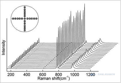
The data has three indicators: the position of the peak, the height of the peak (light intensity), and the width of the peak. Only when the peak position is completely matched, can it be 4H-SiC yang berkelayakan. Seperti XRD, setiap kali terdapat puncak lain, itu adalah zat fasa lain, yang merupakan suatu kekurangan.
The difference in the position of the peak is due to the difference in the energy of the phonons brought about by the different silicon carbide crystal lattices, that is, the different frequencies. Each phonon has its corresponding energy level. The virtual energy level theory can be used to explain Raman (non-linear process):
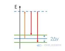
Zarah menyerap cahaya kejadian ke tahap tenaga maya (oren), dan kemudian beralih ke tahap tenaga getaran (merah) yang berbeza dari tahap tenaga asal. Oleh kerana tahap tenaga atas adalah tahap tenaga maya, frekuensi cahaya kejadian boleh berubah-ubah, selagi tidak bertentangan dengan tahap tenaga sebenar yang asal.
Perlu diingat bahawa mod LOPC (964.769 cm-1) dapat digunakan untuk menganalisis kepekatan pembawa:
n = 1.25 * 1017cm-2 *(964.769cm-1-VLOPC measurement)
As the carrier concentration increases, the interaction between atoms and the lattice increases, which makes the Raman peak blue shift (smaller), the intensity decreases, and the width increases. This method is not as accurate as other methods and can only be used as an aid to analyze the silicon carbide crystal distribution.
3. Why not Use XRD to Measure Silicon Carbide Crystal Distribution?
X-rays are optical radiation generated by the transition of electrons in the inner layer of atoms under the bombardment of high-speed moving electrons, including continuous X-rays and characteristic X-rays. Silicon carbide single crystal can be used as X-ray gratings, and the coherent scattering produced by these large numbers of particles (atoms, ions, or molecules) will cause light interference, increasing or decreasing the intensity of scattered X-rays. Due to the superposition of scattered waves from a large number of particles, the beams that interfere with each other to produce the highest intensity are called X-ray diffraction lines.
Untuk memenuhi keadaan difraksi, formula Bragg boleh digunakan: 2dsinθ = nλ.
Rasuk kejadian menyebabkan setiap penyebar dapat memancarkan kembali sebahagian kecil dari intensitinya sebagai gelombang sfera. Sekiranya penyebar disusun secara simetri dengan selang d, gelombang sfera ini hanya akan disegerakkan ke arah di mana perbezaan panjang jalurnya 2dsinθ sama dengan gandaan bilangan bulat panjang gelombang λ. Dalam kes ini, sebahagian rasuk kejadian terpesong oleh sudut 2θ, yang akan menghasilkan titik pantulan dalam corak difraksi.
Use X-rays of known wavelengths to measure the θ angle to calculate the interplanar spacing d, which is used for X-ray structure analysis; the other is to use a silicon carbide seed crystal with a known d to measure the θ angle to calculate the characteristic X-ray wavelength, and then the elements contained in the sample can be found in the existing data.
The measurement formula is 2dSinθ=λ. While the d value among the cubic silicon carbide crystal is close, and the characteristic is not obvious enough, the accurate silicon carbide crystal distribution cannot be precisely determined. For these reasons, it is not suitable to use the XRD to measure the distribution of silicon carbide crystals.

Untuk maklumat lebih lanjut, sila hubungi kami melalui e-mel di victorchan@powerwaywafer.com dan powerwaymaterial@gmail.com.