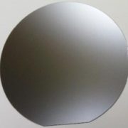
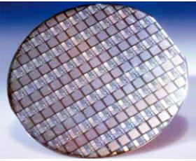
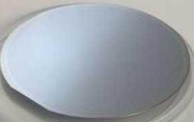
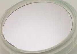
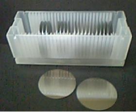
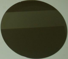
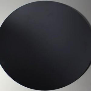
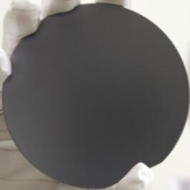
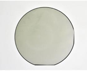
InSb oblea
PAM-XIAMEN offers Compound Semiconductor InSb wafer – Indium antimonide wafer which is grown by LEC(Liquid Encapsulated Czochralski) as epi-ready or mechanical grade with n type, p type or semi-insulating in different orientation(111) or (100). Indium antimonide doped with isoelectronic(such as N doping) can reduce the defect density during the indium antimonide thin films manufacturing process.
- Descripción
Descripción del Producto
PAM-XIAMEN offers Compound Semiconductor InSb wafer – antimonide de indio wafer which is grown by LEC(Liquid Encapsulated Czochralski) as epi-ready or mechanical grade with n type, p type or semi-insulating in different orientation(111) or (100). Indium antimonide doped with isoelectronic(such as N doping) can reduce the defect density during the indium antimonide thin films manufacturing process.
Indium antimonide (InSb) is a crystalline compound made from the elements indium (In) and antimony (Sb). It is a narrow-gap semiconductor material from the III-V group used in infrared detectors, including thermal imaging cameras, FLIR systems, infrared homing missile guidance systems, and in infrared astronomy. The indium antimonide detectors are sensitive between 1–5 µm wavelengths. Indium antimonide was a very common detector in the old, single-detector mechanically scanned thermal imaging systems. Another application is as a terahertz radiation source as it is a strong photo-Dember emitter.
| Especificación de la oblea | |
| Artículo | Especificaciones |
| Diámetro de la oblea | 2 "50,5 ± 0,5 mm |
| 3″76.2±0.4mm | |
| 4″1000.0±0.5mm | |
| cristal Orientación | 2 "(111) AorB ± 0,1 ° |
| 3″(111)AorB±0.1° | |
| 4″(111)AorB±0.1° | |
| Espesor | 2 "625 ± 25um |
| 3″ 800or900±25um | |
| 4″1000±25um | |
| longitud plana primaria | 2 "16 ± 2 mm |
| 3″22±2mm | |
| 4″32.5±2.5mm | |
| longitud plana Secundaria | 2 "8 ± 1 mm |
| 3″11±1mm | |
| 4″18±1mm | |
| Acabado de la superficie | P / E, P / P |
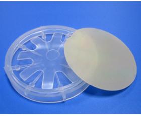
| Paquete | Epi-Ready, recipiente de rebanada única o casete CF |
| Eléctricos y Dopaje Especificación | |||||
| Tipo de conducción | de tipo n | de tipo n | de tipo n | de tipo n | p-tipo |
| dopante | low doped | Telurio | bajo el telurio | alta teluro | Genmanium |
| EPD cm-2 | 2″3″4″≤50 | 2″≤100 | |||
| Mobility cm² V-1s-1 | ≥4*105 | ≥2.5*104 | ≥2.5*105 | No Especificado | 8000-4000 |
| Carrier Concentration cm-3 | 5*1013-3*1014 | (1-7)*1017 | 4*1014-2*1015 | ≥1*1018 | 5*1014-3*1015 |
.png)
1)2″(50.8mm)InSb Wafer
Orientation:(100)
Type/Dopant:N/low doped
Diameter:50.8mm
Thickness:300±25µm;500um
Nc:<2E14a/cm3
Polish:SSP
2)2″(50.8mm)InSb Wafer
Orientation:(100)
Type/Dopant:N/Te
Diameter:50.8mm
Carrier Concentration: 0.8 – 2.1 x 1015 cm-3
Thickness:450+/- 25 um;525±25µm
EPD < 200 cm-2
Polish:SSP
3)2″(50.8mm)InSb Substrate
Orientation:(111) + 0.5°
Thickness:450+/- 50 um
Type/Dopant:N/low doped
Carrier Concentration: < 5 x 10^14 cm-3
EPD < 5 x 103 cm-2
Surface roughness: < 15 A
Bow/Warp: < 30 um
Polish:SSP
4)2″(50.8mm)InSb Substrate
Orientation:(111) + 0.5°
Type/Dopant:P/Ge
Polish:SSP
5)2″(50.8mm)Indium Antimonide Wafer
Thickness:525±25µm,
Orientation:[111A]±0.5°
Type/Dopant:N/Te
Ro=(0.020-0.028)Ohmcm,
Nc=(4-8)E14cm-3/cc,
u=(4.05E5-4.33E5)cm²/Vs,
EPD<100/cm²,
Mobility:>1E4cm2/Vs
One side edge;
In(A) Face: Chemically-mechanically final polished to 0.1µm (Final Polish),
Sb(B) Face: Chemically-mechanically final polished to <5µm (Lasermark),
NOTE: Nc and Mobility are at 77ºK.
Polish:SSP;DSP
6) 2 "(50,8 mm) GaSb
Thickness:525±25µm,
Orientation:[111B]±0.5°,
Type/Dopant:P/low doped;N/low doped
Polish:SSP;DSP
Condición de la superficie y otra especificación
Indium Antimonide wafer can be offered as wafers with as-cut, etched or polished finishes with wide range of doping concentration and thickness. The InSb wafer could be high quality epi-ready finishing.
Especificación de la orientación
Indium antimonide surface orientations are supplied to an accuracy of +/- 0.5 degrees using a triple axis X-Ray diffractometer system. Indium antimonide substrates can also be supplied with very precise misorientations in any direction from the growth plane. The available InSb wafer orientation could be (100),(111), (110) or other orientation or mis degree.
cONDICIONES DE ENVASADO
Polished wafer: individually sealed in two outer bags in inert atmosphere. Cassette shipments are available if required.
As-cut Wafer: Cassette shipment. (Glassine bag available on request).
Indium Antimonide Properties and Uses
The indium antimonide crystal structure is silver, brittle, and zinc blende structure. The indium antimonide lattice constant is 6.48 Å, and indium antimonide is a direct bandgap material with a narrow band gap of 0.18 eV. The indium antimonide conduction electron mobility is as high as 7800 cm2/V·s , which can be used to make infrared detectors, photomagnetic detectors and Hall devices.
Productos relativos:
oblea de InAs
oblea de InSb
oblea de InP
GaAs oblea
GaSb oblea
GaP oblea
Sensor magnetorresistivo diferencial

