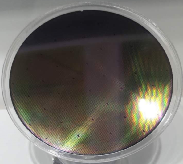
Epi Wafer für Laserdiode
GaAs based LD epitaxy wafer, which can generate stimulate emission, is widely used for fabricating laser diode since the superior GaAs epitaxial wafer properties make the device a low energy consumption, high efficiency, long lifetime and etc. In addition to gallium arsenide LD epi wafer, commonly used semiconductor materials are cadmium sulfide (CdS), indium phosphide (InP), and zinc sulfide (ZnS).
- Beschreibung
Produktbeschreibung
Xiamen Powerway Advanced Material Co., Ltd (PAM-XIAMEN), a LD epitaxial wafer supplier, focuses on the GaAs and InP based laser diode epi wafers grown by MOCVD reactors for fiber-optic communication, industrial application, and special-purpose usage. PAM-XIAMEN can offer LD epitaxy wafer based on GaAs substrate for various fields, like VCSEL, infrared, photo-detector and etc. More details about the LD epitaxy wafer material, please refer to the table below:
| Substratmaterial | Materialfähigkeit | Wellenlänge | Anwendung |
| GaAs | GaAs / GalnP / AlGaInP / GaInP | 635nm | |
| GaAs-basierter Epi-Wafer | 650 nm | Oberflächenemittierender Laser mit vertikalem Hohlraum (VCSEL) RCLED |
|
| GaAs / GalnP / AlGaInP / GaInP | 660 nm | ||
| GaAs / AlGaAs / GalnP / AlGaAs / GaAs | 703 nm | ||
| GaAs / GalnP / AlGaInP / GaInP | 780 nm | ||
| GaAs / GalnP / AlGaInP / GaInP | 785 nm | ||
| GaAs-basierter Epi-Wafer | 800-1064 nm | Infrarot-LD | |
| GaAs / GalnP / AlGaInP / GaInP | 808 nm | Infrarot-LD | |
| GaAs-basierter Epi-Wafer | 850nm | Oberflächenemittierender Laser mit vertikalem Hohlraum (VCSEL) RCLED |
|
| GaAs-basierter Epi-Wafer | <870 nm | Fotodetektor | |
| GaAs-basierter Epi-Wafer | 850-1100 nm | Oberflächenemittierender Laser mit vertikalem Hohlraum (VCSEL) RCLED |
|
| GaAs / AlGaAs / GaInAs / AlGaAs / GaAs | 905nm | ||
| GaAs / AlGaAs / InGaAs / AlGaAs / GaAs | 950 nm | ||
| GaAs-basierter Epi-Wafer | 980nm | Infrarot-LD | |
| InP-basierter Epi-Wafer | 1250-1600 nm | Lawinen-Fotodetektor | |
| GaAs-basierter Epi-Wafer | 1250-1600 nm /> 2,0 um (InGaAs Absorptionsschicht) |
Fotodetektor | |
| GaAs-basierter Epi-Wafer | 1250-1600 nm / <1,4 um (InGaAsP-Absorptionsschicht) |
Fotodetektor | |
| InP-basierter Epi-Wafer | 1270-1630nm | DFB-Laser | |
| GaAsP / GaAs / GaAs-Substrat | 1300nm | ||
| InP-basierter Epi-Wafer | 1310nm | FP-Laser | |
| GaAsP / GaAs / GaAs-Substrat | 1550 nm | FP-Laser | |
| 1654nm | |||
| InP-basierter Epi-Wafer | 1900nm | FP-Laser | |
| 2004nm |
About LD Epitaxy Wafer Applications & Market
The applications of GaAs based LD epitaxy wafer in the laser field can be divided into VCSELs and non-VCSELs. The current GaAs based LD epitaxy applications mainly lies in VCSELs. VCSEL (Vertical Cavity Surface Emitting Laser), based on GaAs materials, is mainly used for face recognition. It is expected to have a high growth rate in the future. EEL (Edge Emitting Laser) is a non-VCSEL device, mainly used in the field of automotive lidar, and the demand is expected to increase with the expansion of the driverless car market.
The GaAs substrate used in the laser field requires high technical indicators, and the unit epitaxial wafer price is significantly higher than that of other fields. The future LD epitaxial market space can be expected. Laser applications are the most sensitive to dislocation density. There is a high requirement for the GaAs substrate materials in laser applications. Therefore, the higher requirement is put forward on LD epitaxial wafer manufacturers and LD epitaxial wafer process. At present, the near-infrared band (760~1060 nm) semiconductor laser based on GaAs substrate has the most mature development and the most widespread application, and it has already been commercialized.
Remark:
The Chinese government has announced new limits on the exportation of Gallium materials (such as GaAs, GaN, Ga2O3, GaP, InGaAs, and GaSb) and Germanium materials used to make semiconductor chips. Starting from August 1, 2023, exporting these materials is only allowed if we obtains a license from the Chinese Ministry of Commerce. Hope for your understanding and cooperation!
Please see below detail specification of LD epitaxy wafer:
GaAs Epitaxy with Thick Growth
GaAs based Epi Structure MOCVD Grown for Light Emitter
Schmales InGaAsP-Quantum-Well-Wachstum auf InP-Wafer
InAs Quantum Dot Layers on InP Substrate
Einzelemitter-Chips
Einzelemitter-LD-Chip 755 nm bei 8 W.
Single-Emitter-LD Chip 808nm @ 8W
Einzelemitter-LD-Chip 808 nm bei 10 W.
Einzelemitter-LD-Chip 830 nm bei 2 W.
Einzelemitter-LD-Chip 880 nm bei 8 W.
Einzelemitter-LD-Chip 900 + nm bei 10 W.
Einzelemitter-LD-Chip 900 + nm bei 15 W.
Einzelemitter-LD-Chip 905 nm bei 25 W.
Einzelemitter-LD-Chip 1470 nm bei 3 W.
PAM XIAMEN bietet 1470 / 1550nm Hochleistungslaser-Einzelchip wie folgt an:
LD Bare Bar
LD Bare Bar für 780nm @ Hohlraum 2.5mm
LD Bare Bar für 808nm @ Hohlraum 2mm
LD Bare Bar für 808nm @ Hohlraum 1,5mm
LD Bare Bar für 880 nm @ Hohlraum 2 mm
LD Bare Bar für 940nm @ Hohlraum 2mm
LD Bare Bar für 940nm @ Hohlraum 3mm
LD Bare Bar für 940nm @ Hohlraum 4mm
LD Bare Bar für 940nm @ Hohlraum 2mm
LD Bare Bar für 976nm @ Hohlraum 4mm