Lithium niobate (LiNbO3) wafer has excellent electro-optic, nonlinear and piezoelectric properties. With the advanced micro- and nanofabrication techniques, integrated photonics devices based on lithium niobate on insulator (LNOI) thin films have been extensively studied. In the future, high-performance LiNbO3 thin film prepared will support the further development of LNOI-based micro-nano optics, integrated photonics, and microwave photonics. The production of high-performance LNOI wafer will be an important part of the industrial application of lithium niobate optoelectronic devices. 4″ LiNbO3 thin film on Silicon Wafer (LNOI) with Y-cut and Z-cut can be provided by PAM-하문 as follows:
1. Specifications of Si-Based Single-Crystal LiNbO3 Thin Film
No.1:
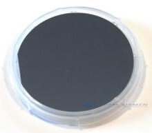
LiNbO3/Silicon Wafer (PAM-P19446-LNOI)
Good Description: Lithium Niobate layer on Silicon Wafer with No Interlayer:LN thin film on Si Wafer
최상층 : 리튬 니오브 산 단결정 박막, Y- 컷, 두께 5μm
기판 : 4 ″ 실리콘 웨이퍼, 두께 0.5mm
High Resistivity >10,000Ω*cm for silicon substrate
표면 거칠기 <0.5nm
두께 균일 성 <2μm, 배송시 17 점 테스트 제공
No.2:
Top layer LiNbO3 thin film Z-cut thickness 300nm Middle layer: (PAM-P20442-LNOI)
Thermal oxide, 2000 nm
Substrate: 4 inch Si wafer, high resistivity≥10,000Ω*cm for Si substrate currently
No.3:
Top layer LiNbO3 thin film Z-cut thickness 400nm Middle layer: (PAM-P20442-LNOI)
Thermal oxide, 2000 nm
Substrate: 4 inch Si wafer, high resistivity≥10,000Ω*cm for Si substrate currently
No.4:
Top layer LiNbO3 thin film Z-cut thickness 500nm Middle layer: (PAM-P20442-LNOI)
Thermal oxide, 2000 nm
Substrate: 4 inch Si wafer, high resistivity≥10,000Ω*cm for Si substrate currently
X-cut LNOI wafer also can be offered, more detailed parameters please consult at victorchan@powerwaywafer.com.
2. Property Comparison between LN and Si
Thin films of Lithium niobate are one of the most widely used optoelectronic materials with outstanding electro-optic properties. LiNbO3 thin film modulator is the backbone of modern optical fiber communication technology. And its transparent window range, optical loss, nonlinear performance, high-speed electro-optic modulation performance and LiNbO3 thin film piezoelectric performance have great advantages over silicon, refer to table 1:
|
Table 1 Performance Comparison Between LN and Si |
||||||
| Materials | Bandgap & Transparent Window | Refractive Index | Electro-optic Coefficient (pm/V) | Second-order:dij (pm/V) | Waveguide Losses | Piezoelectricity |
| 시 | 1.1 eV
1.1-5.5 um |
3.5 | Carrier plasma effect | NA | ~1 dB/cm | NA |
| LN | 4eV
0.35-5.5 um |
2.2 | r33=30.8(Pockels effect | d33=25.2(@1.06um) | ~0.027 dB/cm | d15=74 |
3. FAQ about LiNbO3 Thin Film on Silicon
Q1: We have one more question about the sample. It has two facets: a) with edge trimming and b) with a number – XCP10010005919.
According to the figure you sent the LN layer is placed on the side a) with the edge trimming. The side b) according to the figure is Si. But the side b) looks like an unpolished Si covered with some polished layer (SiO2 or some other material). Could you please clarify this?
Please find in the attachment three images (on the first one you can see both scattered light from the unpolished Si and reflected from the top surface; on the second one mainly the scattered light from Si; on the third one the mirror like specular reflection from the top surface under oblique incident).


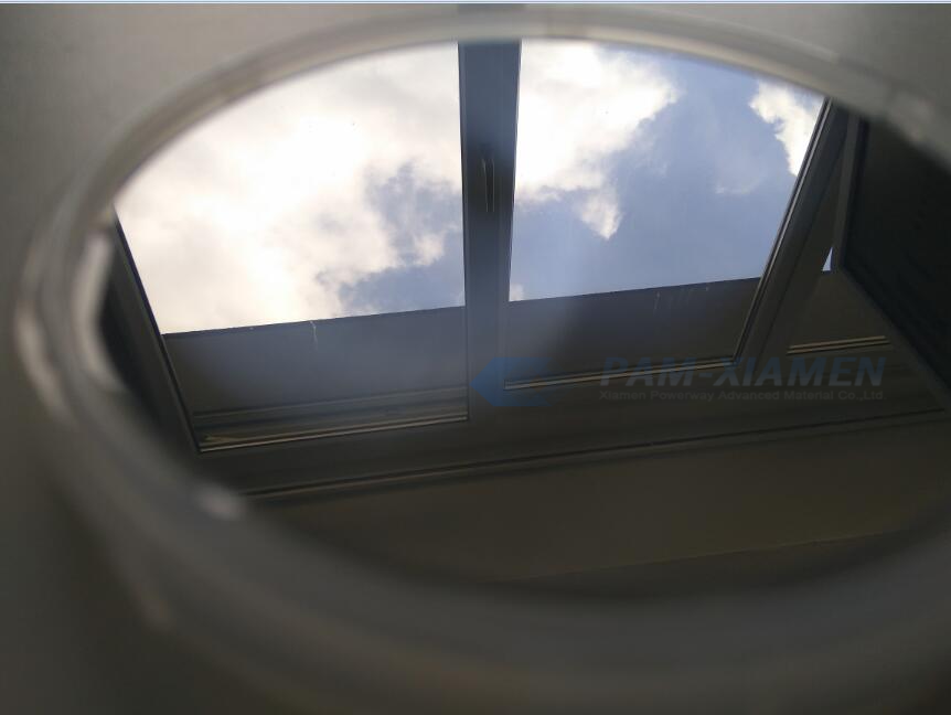
A: The backside of Silicon substrate is ground, and the purpose of grinding is to adjust the TTV of the finished product. The attached picture shows the status of grinding Si substrate on b)side which is not polished, and there is no SiO2 layer.
We bonded the lithium niobate thin film directly to Si substrate, both sides of Si substrate don’t contain silicon dioxide SiO2. The mirror like specular reflection you mentioned should be generated after grinding, it is not the mirror after polishing.
Q2:Is there any optical quality test of the your company LN wafers like refractive index or propagation loss versus wavelength?
A:We have test for the refractive index of LN wafers λ=663nm n0=2.286, ne=2.202.

For more information, please contact us email at victorchan@powerwaywafer.com and powerwaymaterial@gmail.com